ADM1073 Data Sheet
Rev. B | Page 18 of 24
FUNCTIONALITY AND TIMING
LIVE INSERTION
The timing waveforms associated with the live insertion of a
plug-in board using the ADM1073 are shown in Figure 36. The
long connector pins are the first to make connection, and the
GND − V
EE
potential climbs to 48 V. As this voltage is applied,
the voltage at the V
IN
pin ramps to a constant 12.3 V and is held
at this level with the shunt resistor and external resistor
combination at the V
IN
pin. In this case, the connection pins are
staggered so that the R1/R2 and R3/R4 resistor dividers are the
last to connect to the backplane. This means that V
UV
and V
OV
begin to ramp after the other pins connect. Note that staggered
connector pins are optional, because an internal time filter is
included on the UV pin.
When V
UV
crosses the undervoltage rising threshold, it is now
inside the operating voltage window and the −48 V supply must
be applied to the load. The
SPLYGD
output is asserted and after
a time delay, t
POR
, the ADM1073 begins to ramp up the gate
drive. When the voltage on the SENSE pin reaches 100 mV (the
analog current limit level), the gate drive is held constant. When
the board capacitance is fully charged, the sense voltage begins
to drop below the analog current limit voltage and the gate
voltage is free to ramp up further. The gate voltage eventually
climbs to its maximum value of 12.3 V and the
PWRGD
output
is asserted. Figure 37 shows some typical startup waveforms.
t
POR
V
LKO
V
UVR
–48V RTN – VEE
V
IN
V
UV
GATE
SENSE
V
OUT
SPLYGD
PWRGD
0
4488-036
Figure 36. Timing Waveforms Associated with a Live Insertion Event
04488-037
Figure 37. Typical Startup Sequence
(Ch1 = GATE; Ch2 = SENSE; Ch3 =
PWRGD
; Ch4 =
SPLYGD
)
OVERVOLTAGE AND UNDERVOLTAGE FAULTS
The waveforms for an overvoltage glitch are shown in Figure 38.
When V
OV
glitches above the overvoltage threshold of 1.93 V, an
overvoltage condition is detected and the GATE voltage is
pulled low. V
OV
begins to drop back toward the operating
voltage window, and the GATE drive is restored when the
overvoltage falling threshold (1.93 V minus preset OV
hysteresis level) is reached. Figure 38 illustrates the ADM1073’s
reactions to an overvoltage condition.
04488-038
Figure 38. Timing Waveforms Associated with an Overvoltage Fault
(Ch1 = GATE; Ch2 = OV; Ch3 =
PWRGD
; Ch 4 =
SPLYGD
)
Data Sheet ADM1073
Rev. B | Page 19 of 24
An undervoltage glitch is dealt with in a similar way. When V
UV
falls below the undervoltage threshold of 0.868 V, th e G AT E
voltage is pulled low. V
UV
begins to rise back toward the
operating voltage window, and the GATE drive is restored when
the undervoltage rising threshold (0.868 V plus preset UV
hysteresis level) is reached. Figure 39 illustrates the ADM1073’s
operation in an undervoltage situation.
04488-039
Figure 39. Timing Waveforms Associated with an Undervoltage Fault
(Ch1 = GATE; Ch2 = UV; Ch3 =
PWRGD
; Ch4 =
SPLYGD
)
SOFT START
The ADM1073 offers a variable soft start feature. The value of
the capacitor on the SS pin sets the ramp rate of the inrush
current profile at startup. Figure 40 to Figure 42 show different
inrush current ramp rates for three SS capacitors.
04488-040
Figure 40. Soft Start Profile with a 0.1 nF Capacitor
(Ch1 = GATE; Ch2 = SENSE)
04488-041
Figure 41. Soft Start Profile with a 1.5 nF Capacitor
(Ch1 = GATE; Ch2 = SENSE)
04488-042
Figure 42. Soft Start Profile with an 8.2 nF Capacitor
(Ch1 = GATE; Ch2 = SENSE)
ADM1073 Data Sheet
Rev. B | Page 20 of 24
CURRENT FAULTS
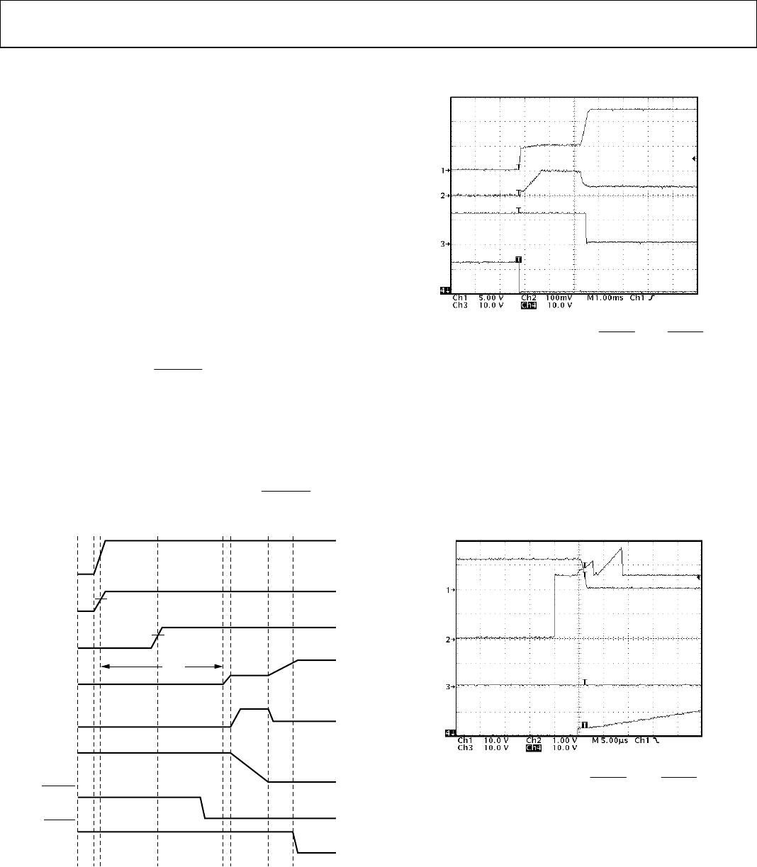
Some timing waveforms associated with overcurrent faults are
shown in the following figures. Figure 43 shows how a perma-
nent current fault is dealt with after startup.
SPLYGD
going low
indicates when the supply voltage is good. Because the output is
shorted, the sense voltage immediately rises through the 90 mV
circuit breaker threshold, and the fault timer is started. The
linear current control loop then goes into regulation at V
SENSE
=
100 mV, accurately limiting the load current at the preset level.
The limited consecutive retry scheme PWMs the GATE pin
seven times. When the seventh retry occurs, the permanent
fault is deemed permanent and the part latches off. The
LATCHED
output asserts at this time. Power must now be
cycled to restart the device. This can be achieved via a manual
card reseating event (which cycles the power) or with an
external
RESTART
or
SHDN
signal.
04488-043
Figure 43. Timing Waveforms Associated with a Current Fault at Startup,
Using Limited Consecutive Retry (Ch1 = GATE; Ch2 = SENSE;
Ch3 =
SPLYGD
; Ch4 =
LATCHED
)
Note that the
LATCHED
output can also be tied back to the
RESTART
input, giving an infinite retry during current fault
with a 5-second cool-down period after every seven retries. The
waveforms for this event are similar to those in
Figure 43, but
repeats every five seconds.
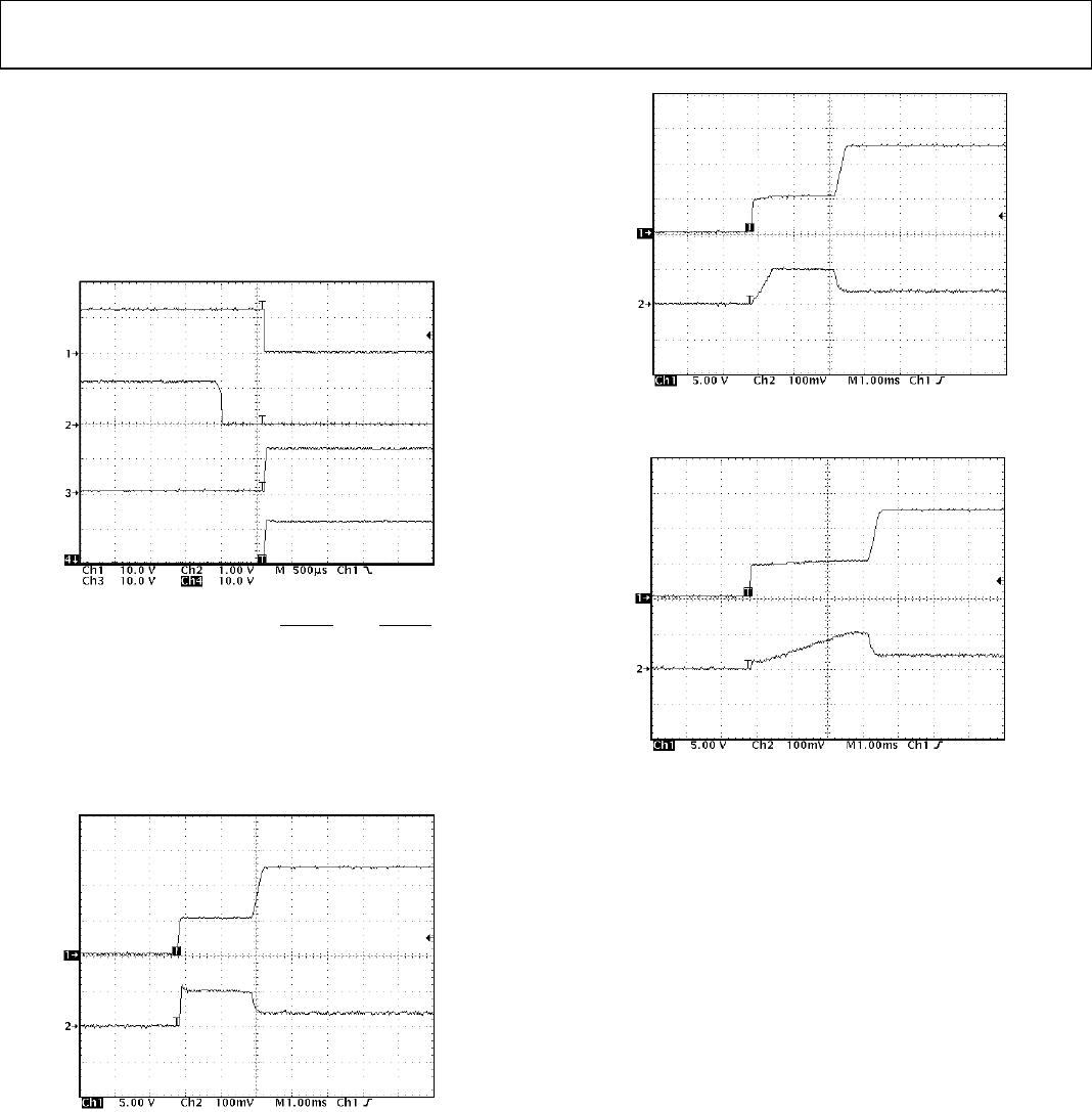
Figure 44 shows the behavior of ADM1073 when a temporary
current fault occurs followed by a permanent current fault.
When the first overcurrent fault occurs, the first 97.5 mV spike
on the SENSE line can be seen. The ADM1073 retries a number
of times, and during the fifth t
OFF
time this current fault corrects
itself. After this time period, a no-fault condition is detected
and the limited consecutive counter is reset. GATE is reasserted.
When the overcurrent fault returns permanently, the limited
consecutive retry counter detects seven consecutive faults and
the part latches off. In this way, the ADM1073 prevents
nuisance shutdowns caused by transient shorts of a
programmable duration (typically ~0.6 s, set via TIMER, as
follows), but provides latched shutdown protection from
permanently shorted loads.
04488-044
Figure 44. Timing Waveforms Associated with a Temporary Current Fault
Followed by a Permanent Current Fault
(Ch1 = GATE; Ch2 = SENSE)
Figure 45 shows the behavior of the TIMER pin during a retry
cycle. Different current sources are switched in during the
on-time (TIMER ramping up) and off-times (TIMER ramping
down). This can be seen in the varying ramp-up and ramp-
down rates of TIMER below. The default ratio of t
ON
to t
OFF
is
6%. This ratio can be reduced with a resistor from TIMER to
V
EE
or increased with a resistor from TIMER to V
IN
. The total
retry period can be extended or reduced by changing the value
of the TIMER capacitor.
04488-045
Figure 45. Timing Waveforms during a Retry Cycle for C
TIMER
= 0.82 nF
(Ch1 = GATE; Ch2 = SENSE; Ch3 = TIMER)

ADM1073ARU-REEL

Mfr. #:
Manufacturer:
Analog Devices Inc.
Description:
Hot Swap Voltage Controllers Full Featured -48V Hot Swap Ctrl'r I.C.
Lifecycle:
New from this manufacturer.
Delivery:
DHL FedEx Ups TNT EMS
Payment:
T/T Paypal Visa MoneyGram Western Union