LT3080-1
10
30801fc
For more information www.linear.com/LT3080-1
temperature and applied voltage. The most common
dielectrics used are specified with EIA temperature char-
acteristic codes of Z5U, Y5V,
X
5R and X7R. The Z5U and
Y5V dielectrics are good for providing high capacitances
in a small package, but they tend to have strong voltage
and temperature coefficients as shown in Figures 2 and 3.
When used with a 5V regulator, a 16V 10µF Y5V capacitor
can exhibit an effective value as low as F to F for the
DC bias voltage applied and over the operating tempera
-
ture range. The X5R and X7R dielectrics result in more
stable characteristics and are more suitable for use as the
output capacitor.
The X
7R type has better stability across
temperature, while the X5R is less expensive and is avail
-
able in higher values. Care still must be exercised when
using X5
R and X7R capacitors; the X5R and X7R codes
only specify operating temperature range and maximum
capacitance change over temperature. Capacitance change
due to DC bias with X5R and X7R capacitors is better than
Y5V and Z5U capacitors, but can still be significant enough
to drop capacitor values below appropriate levels. Capaci
-
tor DC bias characteristics tend to improve as component
case size increases,
but expected capacitance at operating
voltage should be verified.
Voltage and temperature coefficients are not the only
sources of problems. Some ceramic capacitors have a
piezoelectric response. A piezoelectric device generates
voltage across its terminals due to mechanical stress,
similar to the way a piezoelectric microphone works. For a
ceramic capacitor the stress can be induced by vibrations
in the system or thermal transients.
Paralleling Devices
LT3080-1’s may be directly paralleled to obtain higher
output current. The SET pins are tied together and the
IN pins are tied together. This is the same whether its in
three terminal mode or has separate input supplies. The
outputs are connected in common; the internal ballast
resistor equalizes the currents.
The worst-case offset between the SET pin and the output
of only ±2 millivolts allows very small ballast resistors
to be used. As shown in Figure 4, the two devices have
internal ballast resistors, which at full output current gives
better than 90 percent equalized sharing of the current.
The internal resistance of 25 milliohms (per device) only
adds about 25 millivolts of output regulation drop at an
DC BIAS VOLTAGE (V)
CHANGE IN VALUE (%)
30801 F02
20
0
20
40
60
80
–100
0
4
8
10
2 6
12
14
X5R
Y5V
16
BOTH CAPACITORS ARE 16V,
1210 CASE SIZE, 10µF
Figure 2. Ceramic Capacitor DC Bias Characteristics
TEMPERATURE (°C)
50
40
20
0
20
40
60
80
–100
25 75
3080 F03
25 0
50 100 125
Y5V
CHANGE IN VALUE (%)
X5R
BOTH CAPACITORS ARE 16V,
1210 CASE SIZE, 10µF
Figure 3. Ceramic Capacitor Temperature Characteristics
Figure 4. Parallel Devices
applicaTions inFormaTion
+
LT3080-1
V
IN
V
CONTROL
OUT
SET
25mΩ
+
LT3080-1
V
IN
V
IN
4.8V TO 28V
V
OUT
3.3V
2.2A
V
CONTROL
OUT
10µF
F
SET
165k
30801 F04
25mΩ
LT3080-1
11
30801fc
For more information www.linear.com/LT3080-1
output of 2A. At low output voltage, 1V, this adds 2.5%
regulation. The output can be set 19mV high for lower ab-
solute error ±1.3%. Of course, more than two LT3080-1’s
can be paralleled for even higher output current. They are
spread out on the PC board
,
spreading the heat. Input
resistors can further spread the heat if the input-to-output
difference is high.
Thermal Performance
In this example, two LT3080-1 3mm
×
3mm DFN devices
are mounted on a 1oz copper 4-layer PC board. They are
placed approximately 1.5 inches apart and the board is
mounted vertically for convection cooling. Two tests were
set up to measure the cooling performance and current
sharing of these devices.
The first test was done with approximately 0.7V input-
to-output and 1A per device. This gave a 700 milliwatt
dissipation in each device and a 2A output current. The
temperature rise above ambient is approximately 28°C
and both devices were within plus or minus 1°C. Both
the thermal and electrical sharing of these devices is
excellent. The thermograph in Figure 5 shows the tem
-
perature distribution between these devices and the PC
board reaches ambient temperature within about a half
an inch from the devices.
The power is then increased with
1.7V across each de-
vice. This gives 1.7 watts dissipation in each device and
a device temperature of about
90°C,
about 65°C above
ambient as shown in Figure 6. Again, the temperature
matching between the devices is within 2°C, showing
excellent tracking between the devices. The board tem
-
perature has reached approximately 40°
C
within about
0.75 inches of each device.
While 90°C is an acceptable operating temperature for
these devices, this is in 25°C ambient. For higher am-
bients, the temperature must be controlled to prevent
device temperature from exceeding 125°C.
A three meter
per second airflow across the devices will decrease the
device temperature about 20°C providing a margin for
higher operating ambient temperatures.
Both at low power and relatively high power levels de
-
vices can be paralleled for higher output current. Current
sharing and thermal sharing is excellent,
showing that
acceptable operation can be had while keeping the peak
temperatures below excessive operating temperatures on
a board. This technique allows higher operating current
linear regulation to be used in systems where it could
never be used before.
Figure 6. Temperature Rise at 1.7W Dissipation
Figure 5. Temperature Rise at 700mW Dissipation
applicaTions inFormaTion
LT3080-1
12
30801fc
For more information www.linear.com/LT3080-1
Quieting the Noise
The LT3080-1 offers numerous advantages when it comes
to dealing with noise. There are several sources of noise
in a linear regulator. The most critical noise source for any
LDO is the reference; from there, the noise contribution
from the error amplifier must be considered, and the gain
created by using a resistor divider cannot be forgotten.
Traditional low noise regulators bring the voltage refer
-
ence out to an external pin (usually through a large value
resistor) to allow for bypassing and noise reduction of
reference noise. The LT3080-1 does not use a traditional
voltage reference like other linear regulators, but instead
uses a reference current. That current operates with typi-
cal noise current levels of 3.2pA/√Hz (1nA
RMS
over the
10Hz to 100kHz bandwidth). The voltage noise of this is
equal to the noise current multiplied by the resistor value.
The resistor generates spot noise equal to 4kTR (k =
Boltzmann’s constant, 1.38 10
-23
J/°K, and T is absolute
temperature) which is RMS summed with the reference
current noise. To lower reference noise, the voltage set-
ting resistor may be bypassed with a capacitor, though
this causes start-up time to increase as a factor of the RC
time constant.
The LT3080-1 uses a unity-gain follower from the SET pin
to drive the output, and there is no requirement to use
a resistor to set the output voltage. Use a high accuracy
voltage reference placed at the SET pin to remove the er-
rors in output voltage due to reference current tolerance
and resistor tolerance. Active driving of the SET pin is
acceptable; the limitations are the creativity and ingenuity
of the circuit designer.
One problem that a normal linear regulator sees with
reference voltage noise is that noise is gained up along
with the output when using a resistor divider to operate
at levels higher than the normal reference voltage. With
the LT3080-1, the unity-gain follower presents no gain
whatsoever from the SET pin to the output, so noise fig-
ures do not increase accordingly. Error amplifier noise is
typically 125nV/√Hz (40µV
RMS
over the 10Hz to 100kHz
bandwidth); this is another factor that is RMS summed
in to give a final noise figure for the regulator.
Curves in the Typical Performance Characteristics show
noise spectral density and peak-to-peak noise character-
istics for both the reference current and error amplifier
over the 10Hz to 100kHz bandwidth.
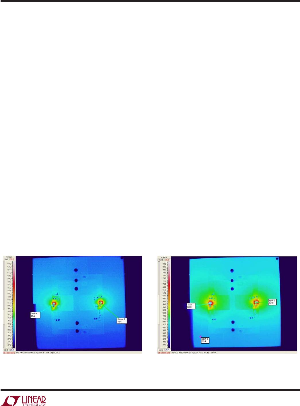
Overload Recovery
Like many IC power regulators, the LT3080-1 has safe oper-
ating area (SOA
) protection
. The SOA protection decreases
current limit as the input-to-output voltage increases and
keeps the power dissipation at safe levels for all values
of input-to-output voltage. The LT3080-1 provides some
output current at all values of input-to-output voltage up
to the device breakdown. See the Current Limit curve in
the Typical Performance Characteristics section.
When power is first turned on, the input voltage rises and
the output follows the input, allowing the regulator to start
into very heavy loads. During start-up, as the input voltage
is rising, the input-to-output voltage differential is small,
allowing the regulator to supply large output currents.
With a high input voltage, a problem can occur wherein
removal of an output short will not allow the output volt
-
age to recover. Other regulators, such as the LT1085 and
LT
1764A,
also exhibit this phenomenon so it is not unique
to the LT3080-1.
The problem occurs with a heavy output load when the
input voltage is high and the output voltage is low. Com
-
mon situations are immediately after the removal of a
short cir
cuit
. The load line for such a load may intersect
the output current curve at two points. If this happens,
there are two stable operating points for the regulator.
With this double intersection, the input power supply may
need to be cycled down to zero and brought up again to
make the output recover.
applicaTions inFormaTion

LT3080EDD-1#PBF

Mfr. #:
Manufacturer:
Analog Devices / Linear Technology
Description:
LDO Voltage Regulators Parallelable 1.1A Adj 1x Res L Drop Reg
Lifecycle:
New from this manufacturer.
Delivery:
DHL FedEx Ups TNT EMS
Payment:
T/T Paypal Visa MoneyGram Western Union