LT3080-1
13
30801fc
For more information www.linear.com/LT3080-1
As output current decreases below the midpoint, output
voltage increases above the nominal set-point. Correspond-
ingly, as output current increases above the midpoint,
output voltage decreases below the nominal set-point
.
During a large output load transient
, output voltage
perturbation is contained within a window that is tighter
than what would result if active voltage positioning is not
employed. Choose the SET pin resistor value by using the
formula below:
R
SET
=
(V
OUT
+
I
MID
R
BALLAST
)
I
SET
where
I
MID
= 1/2 (I
OUT(MIN)
+ I
OUT(MAX)
)
R
BALLAST
= 25mΩ
I
SET
= 10µA
Thermal Considerations
The LT3080-1 has internal power and thermal limiting
circuitry designed to protect it under overload conditions.
For continuous normal load conditions, maximum junc
-
tion temperature must not be exceeded. It is important
to give consideration to all sour
ces of thermal resistance
from junction to ambient
. This includes junction-to-case,
case-to-heat sink interface, heat sink resistance or circuit
board-to-ambient as the application dictates. Additional
heat sources nearby must also be considered.
For surface mount devices, heat sinking is accomplished
by using the heat spreading capabilities of the PC board
and its copper traces. Surface mount heat sinks and plated
through-holes can also be used to spread the heat gener
-
ated by power devices.
Junction-to-case thermal resistance is specified from
the IC junction to the bottom of the case directly below
the die.
This is the lowest resistance path for heat flow.
Proper mounting is required to ensure the best possible
thermal flow from this area of the package to the heat
sinking material. Note that the Exposed Pad is electrically
connected to the output.
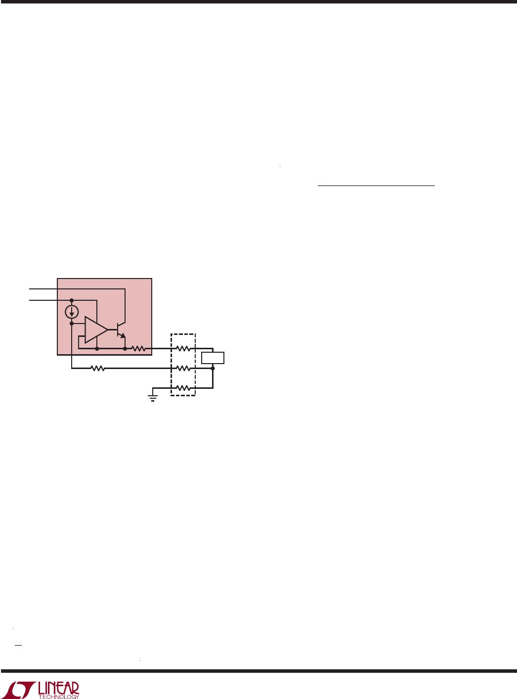
Figure 7. Connections for Best Load Regulation
+
LT3080-1
IN
V
CONTROL
OUT
30801 F07
SET
R
SET
R
P
25mΩ
PARASITIC
RESISTANCE
R
P
R
P
LOAD
Load Regulation
Because the LT3080-1 is a floating device (there is no
ground pin on the part, all quiescent and drive current is
delivered to the load), it is not possible to provide true
remote load sensing. Load regulation will be limited by the
resistance of the connections between the regulator and
the load. The data sheet specification for load regulation
is Kelvin sensed at the pins of the package. Negative side
sensing is a true Kelvin connection, with the bottom of
the voltage setting resistor returned to the negative side of
the load (see Figure 7). Connected as shown, system load
regulation will be the sum of the LT3080-1 load regulation
and the parasitic line resistance multiplied by the output
current. It is important to keep the positive connection
between the regulator and load as short as possible and
use large wire or PC board traces.
applicaTions inFormaTion
The internal 25 ballast resistor is outside of the
LT3080-1’s feedback loop. Therefore, the voltage drop
across the ballast resistor appears as additional DC load
regulation.
However, this additional load regulation can
actually improve transient response performance by de
-
creasing peak-to-peak output voltage deviation and even
save on total output capacitance.
This technique is called
active voltage positioning and is especially useful for ap
-
plications that must withstand large output load current
transients. For more information, see Design Note 224,
Active Voltage Positioning Reduces Output Capacitors.
The basic principle uses the fact that output voltage is
a function of output load current. Output voltage is set
based on the midpoint of the output load current range:
1
2
I
OUT(MIN)
+I
OUT(MAX)
( )
LT3080-1
14
30801fc
For more information www.linear.com/LT3080-1
The following tables list thermal resistance for several
different copper areas given a fixed board size. All mea-
surements were taken in still air on two-sided 1/16"
FR-4
board with one ounce copper.
Table 1. MSE Package, 8-Lead MSOP
COPPER AREA
THERMAL RESISTANCE
(JUNCTION-TO-AMBIENT)
TOPSIDE*
BACKSIDE BOARD AREA
2500mm
2
2500mm
2
2500mm
2
55°C/W
1000mm
2
2500mm
2
2500mm
2
57°C/W
225mm
2
2500mm
2
2500mm
2
60°C/W
100mm
2
2500mm
2
2500mm
2
65°C/W
*Device is mounted on topside
Table 2. DD Package, 8-Lead DFN
COPPER AREA
THERMAL RESISTANCE
(JUNCTION-TO-AMBIENT)
TOPSIDE*
BACKSIDE BOARD AREA
2500mm
2
2500mm
2
2500mm
2
60°C/W
1000mm
2
2500mm
2
2500mm
2
62°C/W
225mm
2
2500mm
2
2500mm
2
65°C/W
100mm
2
2500mm
2
2500mm
2
68°C/W
*Device is mounted on topside
PCB layers, copper weight, board layout and thermal vias
affect the resultant thermal resistance. Although Tables 1
and 2 provide thermal resistance numbers for a 2-layer
board with 1 ounce copper, modern multilayer PCBs pro
-
vide better performance than found in these tables. For
example,
a 4-layer, 1 ounce copper PCB board with five
thermal vias from the DFN or MSOP exposed backside pad
to inner layers (connected to V
OUT
) achieves 40°C/W ther-
mal resistance. Demo circuit 995A’
s board layout achieves
this 40°C/W performance. This is approximately a 33%
improvement over the numbers shown in Tables 1 and 2.
Calculating Junction Temperature
Example: Given an output voltage of 0.9V, a V
CONTROL
voltage of 3.3V ±10%, an IN voltage of 1.5V ±5%, output
current range from 1mA to 1A and a maximum ambient
temperature of 50°C, what will the maximum junction
temperature be for the DFN package on a 2500mm
2
board
with topside copper area of 500mm
2
?
The power in the drive circuit equals:
P
DRIVE
= (V
CONTROL
– V
OUT
)(I
CONTROL
)
where I
CONTROL
is equal to I
OUT
/60. I
CONTROL
is a func-
tion of output current. A curve of I
CONTROL
vs I
OUT
can be
found in the Typical Performance Characteristics curves.
The power in the output transistor equals:
P
OUTPUT
= (V
IN
– V
OUT
)(I
OUT
)
The total power equals:
P
TOTAL
= P
DRIVE
+ P
OUTPUT
The current delivered to the SET pin is negligible and can
be ignored.
V
CONTROL(MAX CONTINUOUS)
= 3.630V (3.3V + 10%)
V
IN(MAX CONTINUOUS)
= 1.575V (1.5V + 5%)
V
OUT
= 0.9V, I
OUT
= 1A, T
A
= 50°C
Power dissipation under these conditions is equal to:
PDRIVE = (V
CONTROL
– V
OUT
)(I
CONTROL
)
I
CONTROL
=
I
OUT
60
=
1A
60
= 17mA
P
DRIVE
= (3.630V – 0.9V)(17mA) = 46mW
P
OUTPUT
= (V
IN
– V
OUT
)(I
OUT
)
P
OUTPUT
= (1.575V – 0.9V)(1A) = 675mW
Total Power Dissipation = 721mW
Junction Temperature will be equal to:
T
J
= T
A
+ P
TOTAL
θ
JA
(approximated using tables)
T
J
= 50°C + 721mW 64°C/W = 96°C
In this case, the junction temperature is below the maxi-
mum rating, ensuring reliable operation.
applicaTions inFormaTion
LT3080-1
15
30801fc
For more information www.linear.com/LT3080-1
Figure 8. Reducing Power Dissipation Using a Series Resistor
+
LT3080-1
IN
V
CONTROL
OUT
V
OUT
V
IN
V
IN
C2
30801 F08
SET
R
SET
25mΩ
R
S
C1
applicaTions inFormaTion
The second technique for reducing power dissipation,
shown in Figure 9, uses a resistor in parallel with the
LT3080-1. This resistor provides a parallel path for current
flow, reducing the current flowing through the LT3080-1.
This technique works well if input voltage is reasonably
constant and output load current changes are small. This
technique also increases the maximum available output
current at the expense of minimum load requirements.
Reducing Power Dissipation
In some applications it may be necessary to reduce
the power dissipation in the LT3080-1 package without
sacrificing output current capability. Two techniques are
available. The first technique, illustrated in Figure 8, em
-
ploys a resistor in series with the regulators input. The
voltage drop
across R
S
decreases the LT3080-1’s IN-to-
OUT differential voltage and correspondingly decreases
the LT3080-1’s power dissipation.
As an example, assume: V
IN
= V
CONTROL
= 5V, V
OUT
= 3.3V
and I
OUT(MAX)
= 1A. Use the formulas from the Calculat-
ing Junction Temperature section previously discussed.
Without series resistor R
S
, power dissipation in the
LT3080-1 equals:
P
TOTAL
= 5V 3.3V
( )
1A
60
+ 5V 3.3V
( )
1A = 1.73
W
If the voltage differential (V
DIFF
) across the NPN pass
transistor is chosen as 0.5V, then R
S
equals:
R
S
=
5V 3.3V
0.5V
1A
= 1.2Ω
Power dissipation in the LT3080-1 now equals:
P
TOTAL
= 5V 3.3V
( )
1A
60
+ 0.5V
( )
1A = 0.53
W
The LT3080-1’s power dissipation is now only 30%
compared to no series resistor. R
S
dissipates 1.2W of
power. Choose appropriate wattage resistors to handle
and dissipate the power properly.
Figure 9. Reducing Power Dissipation Using a Parallel Resistor
+
IN
V
CONTROL
OUT
V
OUT
V
IN
C2
30801 F09
SET
R
SET
R
P
C1
LT3080-1
25mΩ
As an example, assume: V
IN
= V
CONTROL
= 5V, V
IN(MAX)
=
5.5V, V
OUT
= 3.3V, V
OUT(MIN)
= 3.2V, I
OUT(MAX)
= 1A and
I
OUT(MIN)
= 0.7A. Also, assuming that R
P
carries no more
than 90% of I
OUT(MIN)
= 630mA.
Calculating R
P
yields:
R
P
=
5.5V 3.2V
0.63A
= 3.65Ω
(5% Standard value = 3.6Ω)
The maximum total power dissipation is (5.5V – 3.2V)
1A = 2.3W. However, the LT3080-1 supplies only:
1A
5.5V 3.2V
3.6Ω
= 0.36A
Therefore, the LT3080-1’s power dissipation is only:
P
DIS
= (5.5V – 3.2V) 0.36A = 0.83W
R
P
dissipates 1.47W of power. As with the first technique,
choose appropriate wattage resistors to handle and dis-
sipate the power properly. With this configuration, the
LT
3080-1
supplies only 0.36A. Therefore, load current can
increase by 0.64A to 1.64A while keeping the LT3080-1
in its normal operating range.

LT3080EDD-1#PBF

Mfr. #:
Manufacturer:
Analog Devices / Linear Technology
Description:
LDO Voltage Regulators Parallelable 1.1A Adj 1x Res L Drop Reg
Lifecycle:
New from this manufacturer.
Delivery:
DHL FedEx Ups TNT EMS
Payment:
T/T Paypal Visa MoneyGram Western Union