LT3080-1
7
30801fc
For more information www.linear.com/LT3080-1
Output Voltage Noise
Error Amplifier Gain and Phase
FREQUENCY (Hz)
30
GAIN (dB)
PHASE (DEGREES)
–10
20
10k 100k10010 1k 1M
30801 G28
20
0
10
–15
15
25
5
5
–200
0
300
–100
100
200
50
250
–150
50
150
I
L
= 1.1A
I
L
= 100mA
I
L
= 100mA
I
L
= 1.1A
V
CONTROL
(Pin 5/Pin 5): This pin is the supply pin for the
control circuitry of the device. The current flow into this
pin is about 1.7% of the output current. For the device to
regulate, this voltage must be more than 1.2V to 1.35V
greater than the output voltage (see Dropout specifica
-
tions).
IN (
Pins
7, 8/Pins 7, 8): This is the collector to the power
device of the LT3080-1. The output load current is supplied
through this pin. For the device to regulate, the voltage at
this pin must be more than 0.1V to 0.5V greater than the
output voltage (see Dropout specifications).
NC (Pin 6/Pin 6): No Connection. No Connect pins have
no connection to internal circuitry and may be tied to V
IN
,
V
CONTROL
, V
OUT
, GND, or floated.
OUT (Pins 1-3/Pins 1-3): This is the power output of the
device. There must be a minimum load current of 1mA
or the output may not regulate.
SET (Pin 4/Pin 4): This pin is the input to the error am
-
plifier and the regulation set point for the device. A fixed
current of 10µA flows out of this pin through a single
external resistor, which programs the output voltage of
the device. Output voltage range is zero to the absolute
maximum rated output voltage. Transient performance
can be improved by adding a small capacitor from the
SET pin to ground.
Exposed Pad (Pin 9/Pin 9): OUT on MS8E and DFN
packages.
(DD/MS8E)
V
OUT
100µV/DIV
TIME 1ms/DIV
30801 G27
V
OUT
= 1V
R
SET
= 100k
C
SET
= O.1µF
C
OUT
= 10µF
I
LOAD
= 1.1A
Typical perFormance characTerisTics
pin FuncTions
LT3080-1
8
30801fc
For more information www.linear.com/LT3080-1
applicaTions inFormaTion
The LT3080-1 regulator is easy to use and has all the pro-
tection features expected in high performance regulators.
Included are short-circuit protection and safe operating
area protection, as well as thermal shutdown.
The
LT3080-1 is especially well suited to applications
needing multiple rails. The new architecture adjusts down
to zero with a single resistor handling modern low volt
-
age digital ICs as well as allowing easy parallel operation
and thermal management without heat sinks.
Adjusting
to “zero” output allows shutting off the powered circuitry
and when the input is pre-regulatedsuch as a 5V or 3.3V
input supplyexternal resistors can help spread the heat.
A precision “0” TC 10µA internal current source is con
-
nected to the non-inverting input of a power operational
amplifier. The power operational amplifier provides a low
impedance buffered output to the voltage on the non-
inverting input
. A single resistor from the non-inverting
input to ground sets the output voltage and if this resistor
is set to zero, zero output results. As can be seen, any
output voltage can be obtained from zero up to the maxi
-
mum defined by the input power supply.
What is not so obvious from
this architecture are the ben-
efits of using a true internal current source as the reference
as opposed to a bootstrapped reference in older regulators
.
A true current sour
ce allows the regulator to have gain
and frequency response independent of the impedance on
the positive input. Older adjustable regulators, such as the
LT1086 have a change in loop gain with output voltage
as well as bandwidth changes when the adjustment pin
is bypassed to ground. For the LT3080-1, the loop gain is
unchanged by changing the output voltage or bypassing.
Output regulation is not fixed at a percentage of the output
voltage but is a fixed fraction of millivolts. Use of a true
current source allows all the gain in the buffer amplifier
to provide regulation and none of that gain is needed to
amplify up the reference to a higher output voltage.
The LT3080-1 also incorporates an internal ballast resistor
to allow for direct paralleling of devices without the need for
PC board trace resistors or sense resistors. This internal
ballast resistor allows multiple devices to be paralleled
directly on a surface mount board for higher output current
and higher power dissipation while keeping board layout
simple and easy. It is not difficult to add more regulators
for higher output current; inputs of devices are all tied
together, outputs of all devices are tied directly together,
and SET pins of all devices are tied directly together. Be
-
cause of the internal ballast resistor, devices automatically
share the load and the power dissipation.
The
LT3080-1 has the collector of the output transistor
connected to a separate pin from the control input. Since
the dropout on the collector (IN pin) is only 300mV, two
supplies can be used to power the LT3080-1 to reduce
dissipation: a higher voltage supply for the control circuitry
+
V
CONTROL
IN
10µA
25mΩ
30801 BD
OUTSET
block Diagram
LT3080-1
9
30801fc
For more information www.linear.com/LT3080-1
and a lower voltage supply for the collector. This increases
efficiency and reduces dissipation. To further spread the
heat, a resistor can be inserted in series with the collector
to move some of the heat out of the IC and spread it on
the PC board.
The LT3080-1 can be operated in two modes. Three terminal
mode has the control pin connected to the power input pin
which gives a limitation of 1.35V dropout. Alternatively,
the “control” pin can be tied to a higher voltage and the
power IN pin to a lower voltage giving 300mV dropout
on the IN pin and minimizing the power dissipation. This
allows for a 1.1A supply regulating from 2.5V
IN
to 1.8V
OUT
or 1.8V
IN
to 1.2V
OUT
with low dissipation.
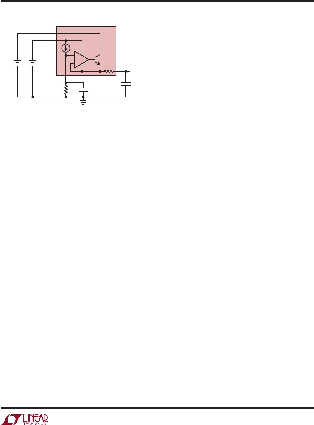
Output Voltage
The LT3080-1 generates a 10µA reference current that
flows out of the SET pin. Connecting a resistor from SET
to ground generates a voltage that becomes the reference
point for the error amplifier (see Figure 1). The reference
voltage is a straight
multiplication of the SET pin current
and the value of the resistor. Any voltage can be generated
and there is no minimum output voltage for the regulator.
A minimum load current of 1mA is required to maintain
regulation regardless of output voltage. For true zero voltage
output operation, this 1mA load current must be returned
to a negative supply voltage.
With the low level current used to generate the reference
voltage, leakage paths to or from the SET pin can create
errors in the reference and output voltages. High quality
insulation should be used (e.g., Teflon, Kel-F); cleaning of all
insulating surfaces to remove fluxes and other residues will
probably be required. Surface coating may be necessary to
provide a moisture barrier in high humidity environments.
Board leakage can be minimized by encircling the SET
pin and circuitry with a guard ring operated at a potential
close to itself; the guard ring should be tied to the OUT
pin. Guarding both sides of the circuit board is required.
Bulk leakage reduction depends on the guard ring width.
Ten nanoamperes of leakage into or out of the SET pin and
associated circuitry creates a 0.1% error in the reference
voltage. Leakages of this magnitude, coupled with other
sources of leakage, can cause significant offset voltage
and reference drift, especially over the possible operating
temperature range.
If guardring techniques are used, this bootstraps any
stray capacitance at the SET pin. Since the SET pin is
a high impedance node, unwanted signals may couple
into the SET pin and cause erratic behavior. This will be
most noticeable when operating with minimum output
capacitors at full load current. The easiest way to remedy
this is to bypass the SET pin with a small amount of ca
-
pacitance from SET to ground, 10pF
to 20pF is sufficient.
Stability and Output Capacitance
The LT3080-1 requires an output capacitor for stability.
It is designed to be stable with most low ESR capacitors
(typically ceramic, tantalum or low ESR electrolytic). A
minimum output capacitor of 2.2µF with an ESR of 0.5Ω
or less is recommended to prevent oscillations.
Larger
values of output capacitance decrease peak
deviations
and provide improved transient response for larger load
current changes. Bypass capacitors, used to decouple
individual components powered by the LT3080-1, increase
the effective output capacitor value.
For improvement in transient performance, place a capaci
-
tor across the voltage setting resistor. Capacitors up to
F can be used. This bypass capacitor reduces system
noise as well, but start-up time is proportional to the time
constant of the voltage setting resistor (R
SET
in Figure 1)
and SET pin bypass capacitor.
Extra consideration must be given to the use of ceramic
capacitors. Ceramic capacitors are manufactured with a
variety of dielectrics, each with different behavior across
Figure 1. Basic Adjustable Regulator
+
LT3080-1
IN
V
CONTROL
V
CONTROL
OUT
30801 F01
SET
C
OUT
R
SET
V
OUT
C
SET
+
V
IN
+
25mΩ
applicaTions inFormaTion

LT3080EDD-1#PBF

Mfr. #:
Manufacturer:
Analog Devices / Linear Technology
Description:
LDO Voltage Regulators Parallelable 1.1A Adj 1x Res L Drop Reg
Lifecycle:
New from this manufacturer.
Delivery:
DHL FedEx Ups TNT EMS
Payment:
T/T Paypal Visa MoneyGram Western Union