1
CAUTION: These devices are sensitive to electrostatic discharge; follow proper IC Handling Procedures.
1-888-INTERSIL or 1-888-468-3774
| Intersil (and design) is a registered trademark of Intersil Americas LLC.
Copyright © Intersil Americas LLC 2003, 2005, 2013, 2015. All Rights Reserved.
All other trademarks mentioned are the property of their respective owners.
82C54
CMOS Programmable Interval Timer
The Intersil 82C54 is a high performance CMOS
Programmable Interval Timer manufactured using an
advanced 2 micron CMOS process.
The 82C54 has three independently programmable and
functional 16-bit counters, each capable of handling clock
input frequencies of up to 8MHz (82C54) or 10MHz
(82C54-10) or 12MHz (82C54-12).
The high speed and industry standard configuration of the
82C54 make it compatible with the Intersil 80C86, 80C88,
and 80C286 CMOS microprocessors along with many
other industry standard processors. Six programmable
timer modes allow the 82C54 to be used as an event
counter, elapsed time indicator, programmable one-shot,
and many other applications. Static CMOS circuit design
insures low power operation.
The Intersil advanced CMOS process results in a significant
reduction in power with performance equal to or greater than
existing equivalent products.
Features
8MHz to 12MHz Clock Input Frequency
Compatible with NMOS 8254
- Enhanced Version of NMOS 8253
Three Independent 16-Bit Counters
Six Programmable Counter Modes
Status Read Back Command
Binary or BCD Counting
Fully TTL Compatible
Single 5V Power Supply
Low Power
- ICCSB. . . . . . . . . . . . . . . . . . . . . . . . . . . . . . . . . . .10µA
- ICCOP . . . . . . . . . . . . . . . . . . . . . . . . . . 10mA at 8MHz
Operating Temperature Ranges
- CX82C54 . . . . . . . . . . . . . . . . . . . . . . . . . 0°C to +70°C
- IX82C54 . . . . . . . . . . . . . . . . . . . . . . . . .-40°C to +85°C
- MD82C54 . . . . . . . . . . . . . . . . . . . . . . .-55°C to +125°C
Pb-Free Plus Anneal Available (RoHS Compliant)
Pinouts
82C54 (PDIP, CERDIP)
TOP VIEW
82C54 (PLCC/CLCC)
TOP VIEW
1
2
3
4
5
6
7
8
9
10
11
12
16
17
18
19
20
21
22
23
24
15
14
13
D7
D6
D5
D4
D3
D2
D1
D0
CLK 0
OUT 0
GATE 0
GND
VCC
RD
CS
A1
A0
OUT 2
CLK 1
GATE 1
OUT 1
WR
CLK 2
GATE 2
GND
NC
OUT 1
GATE 1
CLK 1
OUT 0
GATE 0
D7
NC
VCC
WR
RD
D5
D6
CS
A1
A0
CLK2
NC
GATE 2
OUT 2
1234
5
6
7
8
9
10
11
12 13 14 15 16 17 18
19
20
21
22
23
24
25
262728
D3
D2
D1
D0
D4
NC
CLK 0
Data Sheet FN2970.6September 15, 2015
2
82C54
Ordering Information
PART NUMBERS
TEMP RANGE
(°C) PACKAGE
PKG.
DWG. #8MHz 10MHz 12MHz
CP82C54 CP82C54-10 (No longer available,
recommended replacement:
CP82C54-10Z)
CP82C54-12
(No longer
available,
recommended
replacement:
CP82C54-12Z)
0 to +70 24 Lead PDIP E24.6
CP82C54Z (See Note) CP82C54-10Z (See Note) CP82C54-12Z
(See Note)
0 to +70 24 Lead PDIP** (Pb-free) E24.6
CS82C54* CS82C54-10* CS82C54-12
(No longer
available,
recommended
replacement:
CS82C54-12Z)
0 to +70 28 Lead PLCC N28.45
CS82C54Z* (See Note) CS82C54-10Z* (See Note) CS82C54-12Z*
(See Note)
0 to +70 28 Lead PLCC (Pb-free) N28.45
ID82C54 - - -40 to +85 24 Lead CERDIP F24.6
IP82C54 IP82C54-10 - -40 to +85 24 Lead PDIP E24.6
IP82C54Z (See Note) IP82C54-10Z (See Note) - -40 to +85 24 Lead PDIP** (Pb-free) E24.6
IS82C54* IS82C54-10* - -40 to +85 28 Lead PLCC N28.45
IS82C54Z (See Note) IS82C54-10Z (See Note) - -40 to +85 28 Lead PLCC (Pb-free) N28.45
MD82C54/B - - -55 to +125 24 Lead CERDIP F24.6
SMD # 8406501JA - - -55 to +125 24 Lead CERDIP F24.6
SMD# 84065013A - 84065023A -55 to +125 28 Lead CLCC J28.A
Contact factory for availability.
*Add “96” suffix for tape and reel.
**Pb-free PDIPs can be used for through hole wave solder processing only. They are not intended for use in Reflow solder processing applications.
NOTE: Intersil Pb-free plus anneal products employ special Pb-free material sets; molding compounds/die attach materials and 100% matte tin
plate termination finish, which are RoHS compliant and compatible with both SnPb and Pb-free soldering operations. Intersil Pb-free products are
MSL classified at Pb-free peak reflow temperatures that meet or exceed the Pb-free requirements of IPC/JEDEC J STD-020.
3
82C54
Absolute Maximum Ratings Thermal Information
Supply Voltage. . . . . . . . . . . . . . . . . . . . . . . . . . . . . . . . . . . . . +8.0V
Input, Output or I/O Voltage . . . . . . . . . . . . GND-0.5V to V
CC
+0.5V
ESD Classification . . . . . . . . . . . . . . . . . . . . . . . . . . . . . . . . . Class 1
Operating Conditions
Operating Voltage Range. . . . . . . . . . . . . . . . . . . . . . +4.5V to +5.5V
Operating Temperature Range
CX82C54 . . . . . . . . . . . . . . . . . . . . . . . . . . . . . . . . . 0°C to +70°C
IX82C54 . . . . . . . . . . . . . . . . . . . . . . . . . . . . . . . . .-40°C to +85°C
MD82C54 . . . . . . . . . . . . . . . . . . . . . . . . . . . . . . .-55°C to +125°C
Thermal Resistance (Typical)
JA
(
o
C/W)
JC
(
o
C/W)
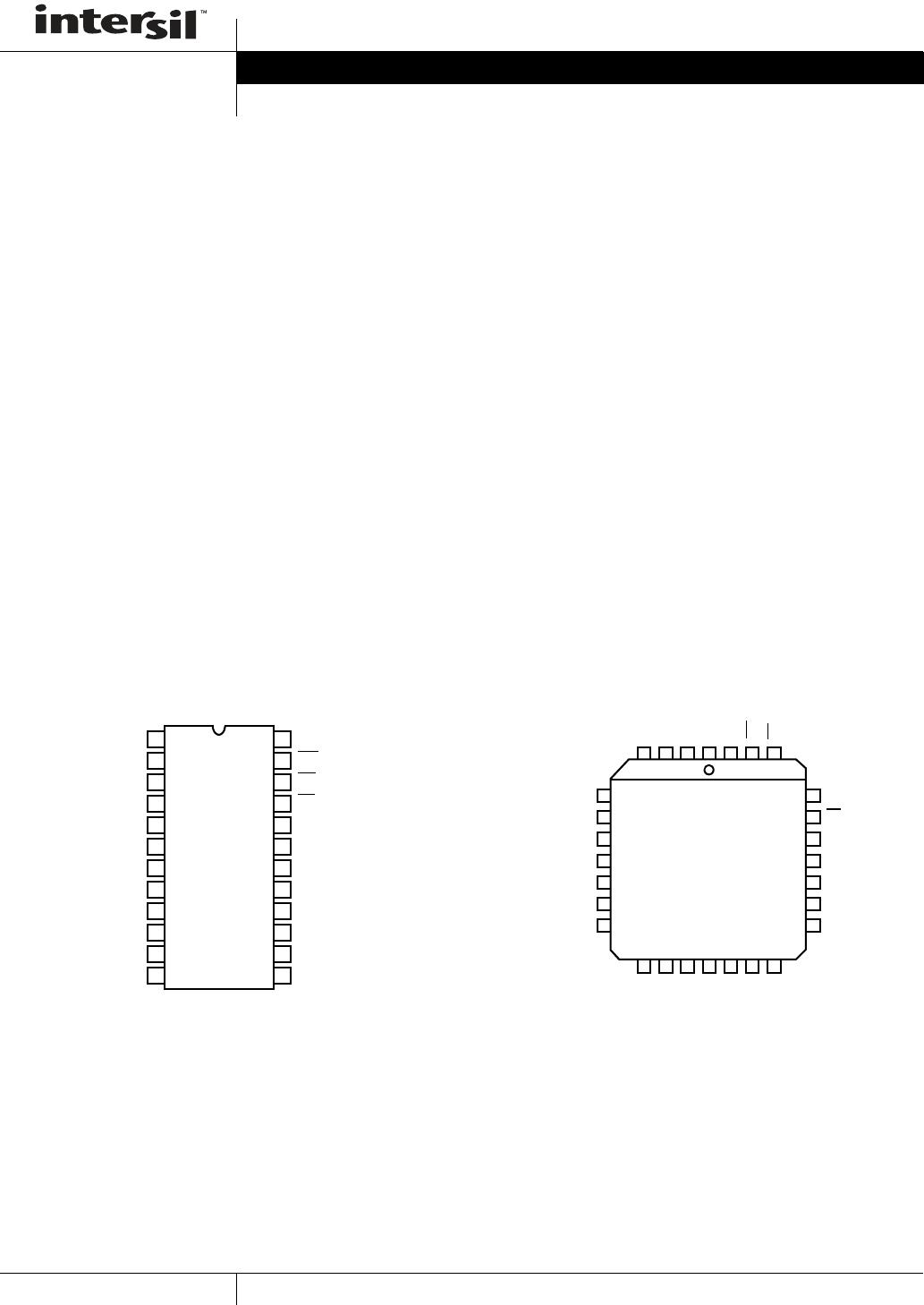
CERDIP Package. . . . . . . . . . . . . . . . . 55 12
CLCC Package . . . . . . . . . . . . . . . . . . 65 14
PDIP Package* . . . . . . . . . . . . . . . . . . 55 N/A
PLCC Package. . . . . . . . . . . . . . . . . . . 60 N/A
Storage Temperature Range . . . . . . . . . . . . . . . . . .-65°C to +150°C
Maximum Junction Temperature Ceramic Package . . . . . . . +175°C
Maximum Junction Temperature Plastic Package. . . . . . . . . +150°C
Maximum Lead Temperature Package (Soldering 10s). . . . . +300°C
(PLCC - Lead Tips Only)
*Pb-free PDIPs can be used for through hole wave solder
processing only. They are not intended for use in Reflow solder
processing applications.
Die Characteristics
Gate Count . . . . . . . . . . . . . . . . . . . . . . . . . . . . . . . . . . .2250 Gates
CAUTION: Stresses above those listed in “Absolute Maximum Ratings” may cause permanent damage to the device. This is a stress only rating and operation of the
device at these or any other conditions above those indicated in the operational sections of this specification is not implied.
DC Electrical Specifications V
CC
= +5.0V ± 10%, Includes all Temperature Ranges
SYMBOL PARAMETER MIN MAX UNITS TEST CONDITIONS
VIH Logical One Input Voltage 2.0 - V CX82C54, IX82C54
2.2 - V MD82C54
VIL Logical Zero Input Voltage - 0.8 V -
VOH Output HIGH Voltage 3.0 - V IOH = -2.5mA
V
CC
-0.4 - V IOH = -100A
VOL Output LOW Voltage - 0.4 V IOL = +2.5mA
II Input Leakage Current -1 +1 A VIN = GND or V
CC
DIP Pins 9,11,14-16,18-23
IO Output Leakage Current -10 +10 A VOUT = GND or V
CC
DIP Pins 1-8
ICCSB Standby Power Supply Current - 10 AV
CC
= 5.5V, VIN = GND or V
CC
,
Outputs Open, Counters
Programmed
ICCOP Operating Power Supply Current - 10 mA V
CC
= 5.5V,
CLK0 = CLK1 = CLK2 = 8MHz,
VIN = GND or V
CC
,
Outputs Open
Capacitance T
A
= +25
o
C; All Measurements Referenced to Device GND, Note 1
SYMBOL PARAMETER TYP UNITS TEST CONDITIONS
CIN Input Capacitance 20 pF FREQ = 1MHz
COUT Output Capacitance 20 pF FREQ = 1MHz
CI/O I/O Capacitance 20 pF FREQ = 1MHz
NOTE:
1. Not tested, but characterized at initial design and at major process/design changes.

CS82C54-10Z

Mfr. #:
Manufacturer:
Renesas / Intersil
Description:
Timers & Support Products PERIPH PRG-CNTR 5V 10MHZ 28PLCC COM
Lifecycle:
New from this manufacturer.
Delivery:
DHL FedEx Ups TNT EMS
Payment:
T/T Paypal Visa MoneyGram Western Union