6.42
IDT7009L
High-Speed 128K x 8 Dual-Port Static RAM Industrial and Commercial Temperature Ranges
3
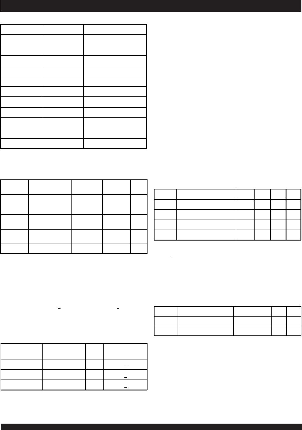
Pin Names
Left Port Right Port Names
CE
0L
, CE
1L
CE
0R
, CE
1R
Chip Enables
R/W
L
R/W
R
Read/Write Enable
OE
L
OE
R
Output Enable
A
0L
- A
16L
A
0R
- A
16R
Address
I/O
0L
- I/O
7L
I/O
0R
- I/O
7R
Data Input/Output
SEM
L
SEM
R
Semaphore Enable
INT
L
INT
R
Interrupt Flag
BUSY
L
BUSY
R
Busy Flag
M/S Master or Slave Select
V
CC
Power
GND Ground
4839 tbl 01
NOTES:
1. This parameter is determined by device characterization but is not production
tested.
2. 3dV represents the interpolated capacitance when the input and output signals
switch from 0V to 3V or from 3V to 0V.
Capacitance
(TA = +25°C, f = 1.0MHz) (TQFP Only)
Absolute Maximum Ratings
(1)
NOTES:
1. Stresses greater than those listed under ABSOLUTE MAXIMUM RATINGS may
cause permanent damage to the device. This is a stress rating only and
functional operation of the device at these or any other conditions above those
indicated in the operational sections of this specification is not implied. Exposure
to absolute maximum rating conditions for extended periods may affect
reliability.
2. V
TERM must not exceed Vcc + 10% for more than 25% of the cycle time or 10ns
maximum, and is limited to
< 20mA for the period of VTERM > Vcc + 10%.
NOTES:
1. V
IL > -1.5V for pulse width less than 10ns.
2. V
TERM must not exceed Vcc + 10%.
Recommended DC Operating
Conditions
NOTES:
1. This is the parameter T
A. This is the "instant on" case temperature.
Maximum Operating Temperature
and Supply Voltage
Symbol Rating Commercial
& Industrial
Military Unit
V
TE RM
(2 )
Terminal Voltage
with Respect
to GND
-0.5 to +7.0 -0.5 to +7.0 V
T
BIAS
Temperature
Under Bias
-55 to +125 -65 to +135
o
C
T
STG
Storage
Temperature
-65 to +150 -65 to +150
o
C
I
OUT
DC Output Current 50 50 mA
4839 tbl 02
Grade
Ambient
Temperature
(2 )
GND Vcc
Military -55
O
C to +125
O
C0V 5.0V
+
10%
Commercial 0
O
C to +70
O
C0V 5.0V
+
10%
Industrial -40
O
C to +85
O
C0V 5.0V
+
10%
4839 tbl 03
Symbol Parameter Min. Typ. Max. Unit
V
CC
Supply Voltage 4.5 5.0 5.5 V
GND Ground 0 0 0 V
V
IH
Input High Voltage 2.2
____
6.0
(2 )
V
V
IL
Input Low Voltage -0.5
(1 )
____
0.8 V
4839 tbl 04
Symbol Parameter
(1 )
Conditions
(2)
Max. Unit
C
IN
Input Capacitance V
IN
= 3dV 9 pF
C
OUT
Output Capacitance V
OUT
= 3dV 10 pF
4839 tbl 05

