DocID025077 Rev 2 17/22
VND5N07-E Protection features
21
3 Protection features
During normal operation, the INPUT pin is electrically connected to the gate of the internal
Power MOSFET.
The device then behaves like a standard Power MOSFET and can be used as a switch from
DC to 50KHz. The only difference from the user’s standpoint is that a small DC current I
ISS
flows into the INPUT pin in order to supply the internal circuitry.
The device integrates:
3.1 Overvoltage clamp protection
Internally set at 70 V, along with the rugged avalanche characteristics of the Power
MOSFET stage give this device unrivaled ruggedness and energy handling capability. This
feature is mainly important when driving inductive loads.
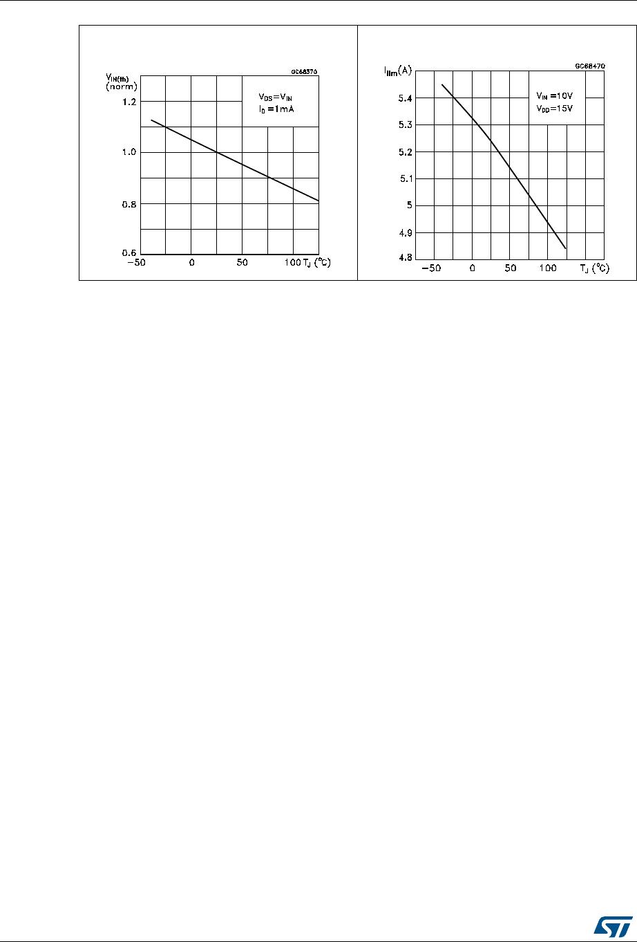
3.2 Linear current limiter circuit
Limits the drain current I
D
to I
lim
whatever the INPUT pin voltages. When the current limiter
is active, the device operates in the linear region, so power dissipation may exceed the
capability of the heatsink. Both case and junction temperatures increase, and if this phase
lasts long enough, junction temperature may reach the overtemperature threshold T
jsh
.
3.3 Overtemperature and short circuit protection
These are based on sensing the chip temperature and are not dependent on the input
voltage. The location of the sensing element on the chip in the power stage area ensures
fast, accurate detection of the junction temperature. Overtemperature cutout occurs at
minimum 150 °C. The device is automatically restarted when the chip temperature falls
below 135 °C.
3.4 Status feedback
In case of an overtemperature fault condition, a Status Feedback is provided through the
Input pin. The internal protection circuit disconnects the input from the gate and connects it
instead to ground via an equivalent resistance of 100 Ω. The failure can be detected by
monitoring the voltage at the Input pin, which will be close to ground potential.
Additional features of this device are ESD protection according to the Human Body model
and the ability to be driven from a TTL Logic circuit (with a small increase in R
DS(on)
).