MAX15012/MAX15013
Applications Information
Supply Bypassing and Grounding
Pay extra attention to bypassing and grounding the
MAX15012/MAX15013. Peak supply and output cur-
rents may exceed 4A when both drivers are driving
large external capacitive loads in-phase. Supply drops
and ground shifts create forms of negative feedback for
inverters and may degrade the delay and transition
times. Ground shifts due to insufficient device ground-
ing may also disturb other circuits sharing the same AC
ground return path. Any series inductance in the V
DD
,
DH, DL, and/or GND paths can cause oscillations due
to the very high di/dt when switching the MAX15012/
MAX15013 with any capacitive load. Place one or more
0.1µF ceramic capacitors in parallel as close to the
device as possible to bypass V
DD
to GND. Use a
ground plane to minimize ground return resistance and
series inductance. Place the external MOSFET as close
as possible to the MAX15012/MAX15013 to further min-
imize board inductance and AC path resistance.
Power Dissipation
Power dissipation in the MAX15012/MAX15013 is pri-
marily due to power loss in the internal boost diode and
the nMOS and pMOS FETs.
For capacitive loads, the total power dissipation for the
device is:
where C
L
is the combined capacitive load at DH and
DL. V
DD
is the supply voltage and f
SW
is the switching
frequency of the converter. P
D
includes the power dis-
sipated in the internal bootstrap diode. The internal
power dissipation reduces by P
DIODE
, if an external
bootstrap Schottky diode is used. The power dissipa-
tion in the internal boost diode (when driving a capaci-
tive load) is the charge through the diode per switching
period multiplied by the maximum diode forward volt-
age drop (V
f
= 1V).
The total power dissipation when using the internal
boost diode is P
D
and, when using an external
Schottky diode, is P
D
- P
DIODE
. The total power dissi-
pated in the device must be kept below the maximum
of 0.471W for the 8-pin SO package at T
A
= +70°C
ambient.
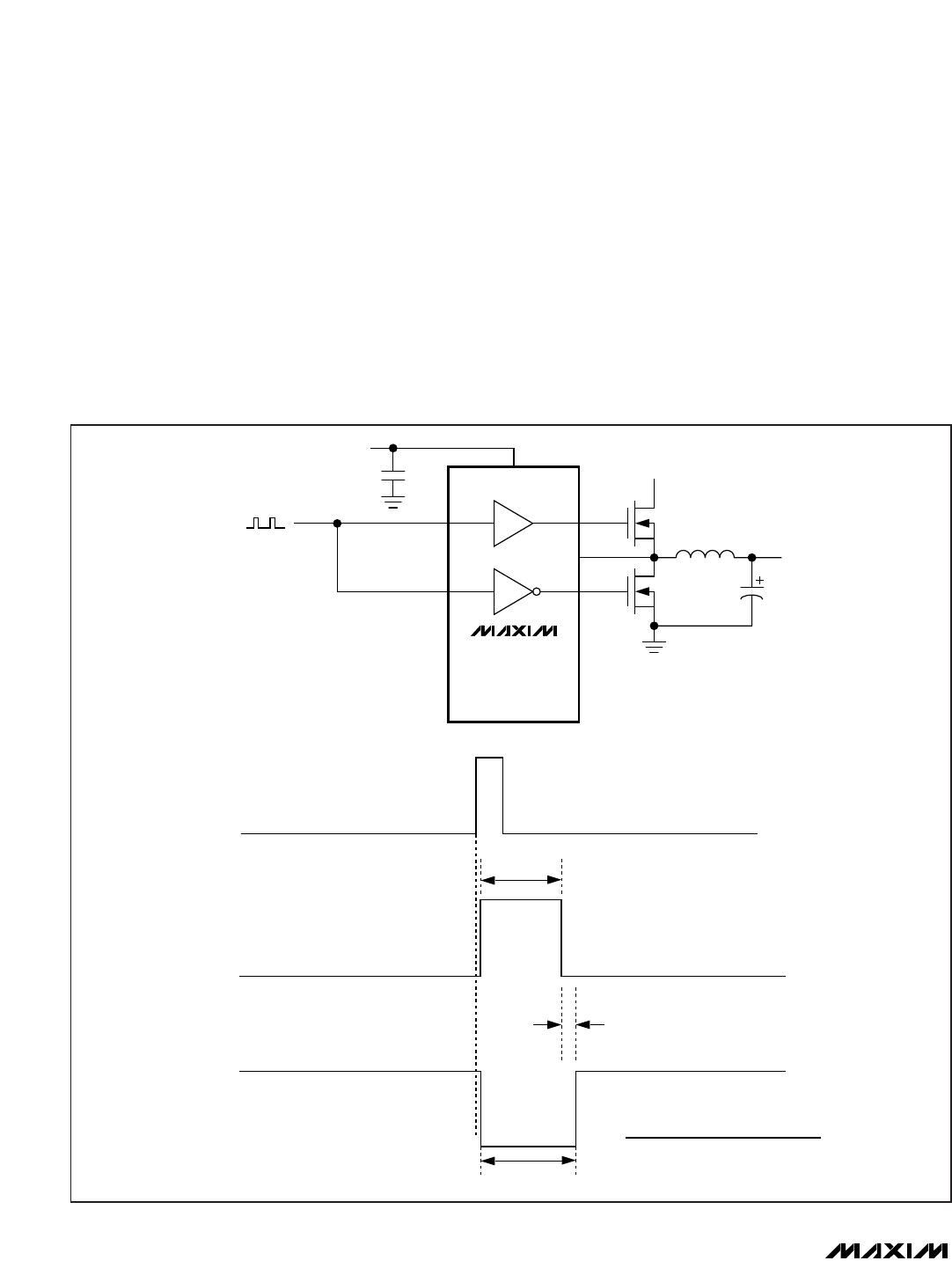
Layout Information
The MAX15012/MAX15013 drivers source and sink
large currents to create very fast rise and fall edges at
the gates of the switching MOSFETs. The high di/dt can
cause unacceptable ringing if the trace lengths and
impedances are not well controlled. Use the following
PC board layout guidelines when designing with the
MAX15012/MAX15013:
• It is important that the V
DD
voltage (with respect to
ground) or BST voltage (with respect to HS) does
not exceed 13.2V. Voltage spikes higher than 13.2V
from V
DD
to GND or BST to HS can damage the
device. Place one or more low ESL 0.1µF decou-
pling ceramic capacitors from V
DD
to GND, and
from BST to HS as close as possible to the part. The
ceramic decoupling capacitors should be at least 20
times the gate capacitance being driven.
• There are two AC current loops formed between the
device and the gate of the MOSFET being driven.
The MOSFET looks like a large capacitance from gate
to source when the gate is being pulled low. The
active current loop is from the MOSFET driver output
(DL or DH) to the MOSFET gate, to the MOSFET
source, and to the return terminal of the MOSFET dri-
ver (either GND or HS). When the gate of the MOSFET
is being pulled high, the active current loop is from
the MOSFET driver output, (DL or DH), to the
MOSFET gate, to the MOSFET source, to the return
terminal of the drivers decoupling capacitor, to the
positive terminal of the decoupling capacitor, and to
the supply connection of the MOSFET driver. The
decoupling capacitor is either the flying capacitor
connected between BST and HS or the decoupling
capacitor for V
DD
. Care must be taken to minimize the
physical length and the impedance of these AC cur-
rent paths.