1
LTC1435
High Efficiency Low Noise
Synchronous Step-Down
Switching Regulator
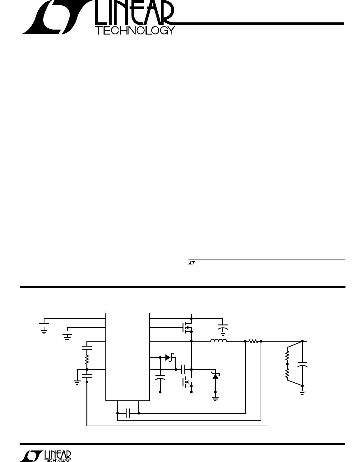
Figure 1. High Efficiency Step-Down Converter
FEATURES
DESCRIPTION
U
Dual N-Channel MOSFET Synchronous Drive
Programmable Fixed Frequency
Wide V
IN
Range: 3.5V to 36V Operation
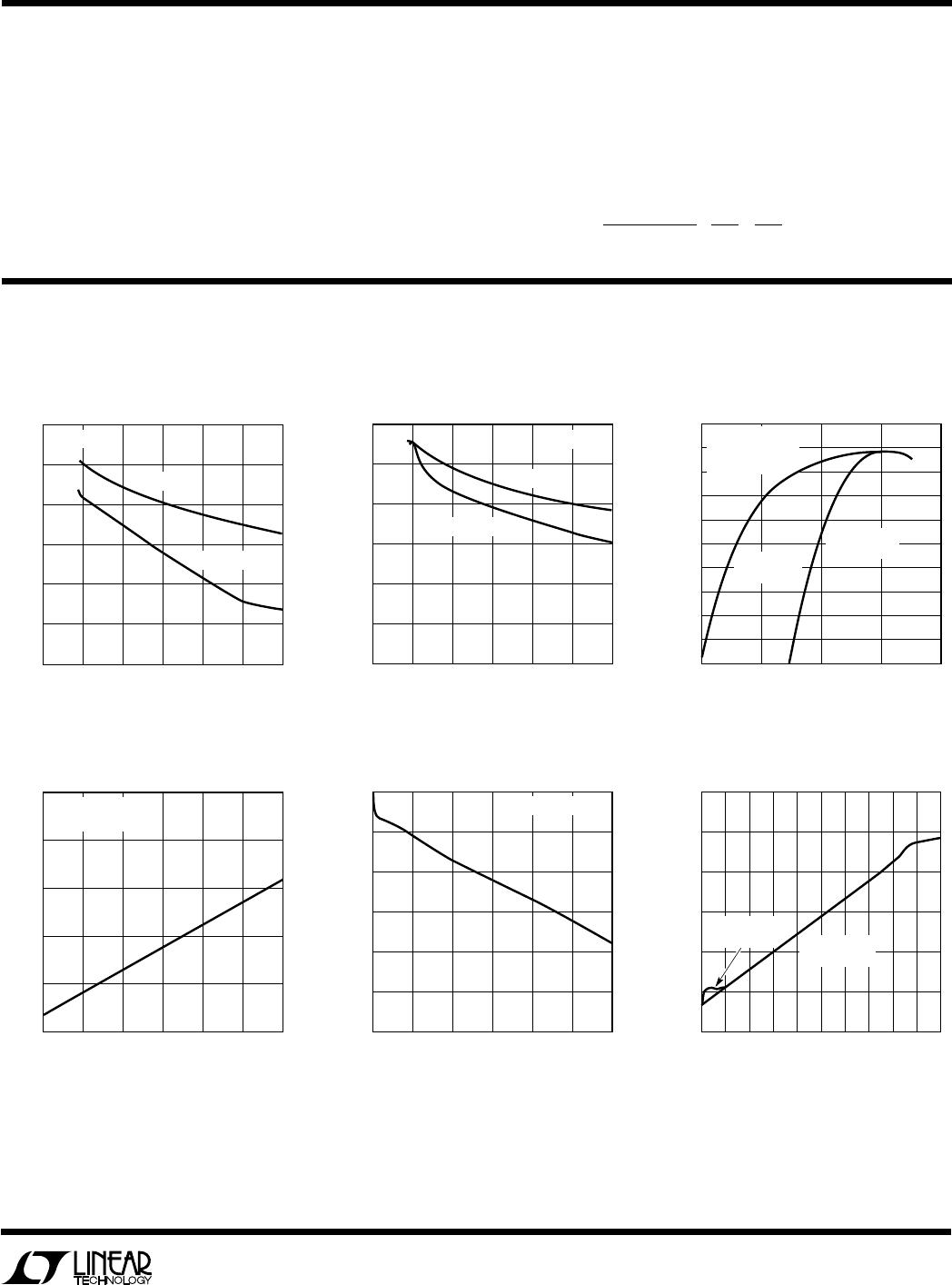
Ultrahigh Efficiency
Very Low Dropout Operation: 99% Duty Cycle
Low Standby Current
Secondary Feedback Control
Programmable Soft Start
Remote Output Voltage Sense
Logic Controlled Micropower Shutdown: I
Q
< 25µA
Foldback Current Limiting (Optional)
Current Mode Operation for Excellent Line and Load
Transient Response
Output Voltages from 1.19V to 9V
Available in 16-Lead Narrow SO and SSOP Packages
The LTC
®
1435 is a synchronous step-down switching
regulator controller that drives external N-channel power
MOSFETs using a fixed frequency architecture. Burst
Mode
TM
operation provides high efficiency at low load
currents. A maximum duty cycle limit of 99% provides low
dropout operation which extends operating time in bat-
tery-operated systems.
The operating frequency is set by an external capacitor
allowing maximum flexibility in optimizing efficiency. A
secondary winding feedback control pin, SFB, guarantees
regulation regardless of load on the main output by
forcing continuous operation. Burst Mode operation is
inhibited when the SFB pin is pulled low which reduces
noise and RF interference.
Soft start is provided by an external capacitor which can
be used to properly sequence supplies. The operating
current level is user-programmable via an external current
sense resistor. Wide input supply range allows operation
from 3.5V to 30V (36V maximum).
, LTC and LT are registered trademarks of Linear Technology Corporation.
Burst Mode is a trademark of Linear Technology Corporation.
Notebook and Palmtop Computers, PDAs
Cellular Telephones and Wireless Modems
Portable Instruments
Battery-Operated Devices
DC Power Distribution Systems
APPLICATIONS
U
TYPICAL APPLICATION
U
I
TH
TG
C
OSC
68pF
C
C
330pF
100pF
R
C
10k
C
SS
0.1µF
SENSE
SENSE
+
LTC1435
1000pF
+
4.7µF
D
B
CMDSH-3
C
B
0.1µF
M2
Si4412DY
D1
MBRS140T3
L1
10µH
M1
Si4412DY
R
SENSE
0.033
+
C
IN
22µF
35V
× 2
V
IN
4.5V TO 28V
+
C
OUT
100µF
10V
× 2
R1
32.4k
R2
22.1k
V
OUT
2.9V/3.5A
PGND
BG
C
OSC
V
IN
V
OSENSE
BOOST
1435 F01
SGND
RUN/SS
SW
INTV
CC
2
LTC1435
ABSOLUTE MAXIMUM RATINGS
W
WW
U
PACKAGE/ORDER INFORMATION
W
U
U
ORDER PART
NUMBER
Input Supply Voltage (V
IN
).........................36V to –0.3V
Topside Driver Supply Voltage (Boost)......42V to –0.3V
Switch Voltage (SW)............................. V
IN
+ 5V to –5V
EXTV
CC
Voltage ........................................ 10V to –0.3V
Sense
+
, Sense
Voltages ......... INTV
CC
+ 0.3V to –0.3V
I
TH
, V
OSENSE
Voltages .............................. 2.7V to –0.3V
SFB, Run/SS Voltages .............................. 10V to –0.3V
Peak Driver Output Current < 10µs (TG, BG)............. 2A
INTV
CC
Output Current ........................................ 50mA
Operating Ambient Temperature Range
LTC1435C............................................... 0°C to 70°C
LTC1435I............................................ 40°C to 85°C
Junction Temperature (Note 1)............................. 125°C
Storage Temperature Range ................. 65°C to 150°C
Lead Temperature (Soldering, 10 sec).................. 300°C
LTC1435CG
LTC1435CS
LTC1435IG
LTC1435IS
T
A
= 25°C, V
IN
= 15V, V
RUN/SS
= 5V unless otherwise noted.
ELECTRICAL CHARACTERISTICS
SYMBOL PARAMETER CONDITIONS MIN TYP MAX UNITS
Main Control Loop
I
IN
V
OSENSE
Feedback Current (Note 2) 10 50 nA
V
OSENSE
Feedback Voltage (Note 2) 1.178 1.19 1.202 V
V
LINEREG
Reference Voltage Line Regulation V
IN
= 3.6V to 20V (Note 2) 0.002 0.01 %/V
V
LOADREG
Output Voltage Load Regulation I
TH
Sinking 5µA (Note 2) 0.5 0.8 %
I
TH
Sourcing 5µA 0.5 0.8 %
V
SFB
Secondary Feedback Threshold V
SFB
Ramping Negative 1.16 1.19 1.22 V
I
SFB
Secondary Feedback Current V
SFB
= 1.5V 1 2 µA
V
OVL
Output Overvoltage Lockout 1.24 1.28 1.32 V
I
Q
Input DC Supply Current EXTV
CC
= 5V (Note 3)
Normal Mode 3.6V < V
IN
< 30V 260 µA
Shutdown V
RUN/SS
= 0V, 3.6V < V
IN
< 15V 16 25 µA
V
RUN/SS
Run Pin Threshold 0.8 1.3 2 V
I
RUN/SS
Soft Start Current Source V
RUN/SS
= 0V 1.5 3 4.5 µA
V
SENSE(MAX)
Maximum Current Sense Threshold V
OSENSE
= 0V, 5V 130 150 180 mV
TG Transition Time
TG t
r
Rise Time C
LOAD
= 3000pF 50 150 ns
TG t
f
Fall Time C
LOAD
= 3000pF 50 150 ns
BG Transition Time
BG t
r
Rise Time C
LOAD
= 3000pF 50 150 ns
BG t
f
Fall Time C
LOAD
= 3000pF 40 150 ns
Internal V
CC
Regulator
V
INTVCC
Internal V
CC
Voltage 6V < V
IN
< 30V, V
EXTVCC
= 4V 4.8 5.0 5.2 V
V
LDO
INT INTV
CC
Load Regulation I
INTVCC
= 15mA, V
EXTVCC
= 4V 0.2 1 %
V
LDO
EXT EXTV
CC
Voltage Drop I
INTVCC
= 15mA, V
EXTVCC
= 5V 130 230 mV
V
EXTVCC
EXTV
CC
Switchover Voltage I
INTVCC
= 15mA, V
EXTVCC
Ramping Positive 4.5 4.7 V
Oscillator
f
OSC
Oscillator Frequency C
OSC
= 100pF (Note 4) 112 125 138 kHz
TOP VIEW
S PACKAGE
16-LEAD PLASTIC SO
G PACKAGE
16-LEAD PLASTIC SSOP
1
2
3
4
5
6
7
8
16
15
14
13
12
11
10
9
C
OSC
RUN/SS
I
TH
SFB
SGND
V
OSENSE
SENSE
SENSE
+
TG
BOOST
SW
V
IN
INTV
CC
BG
PGND
EXTV
CC
T
JMAX
= 125°C, θ
JA
= 130°C/ W (G)
T
JMAX
= 125°C, θ
JA
= 110°C/ W (S)
Consult factory for Military grade parts.
3
LTC1435
ELECTRICAL CHARACTERISTICS
The denotes specifications which apply over the full operating
temperature range.
LTC1435CG/LTC1435CS: 0°C T
A
70°C
LTC1435IG/LTC1435IS: –40°C T
A
85°C
Note 1: T
J
is calculated from the ambient temperature T
A
and power
dissipation P
D
according to the following formula:
LTC1435CG/LTC1435IG: T
J
= T
A
+ (P
D
)(130°C/W)
LTC1435CS/LTC1435IS: T
J
= T
A
+ (P
D
)(110°C/W)
Note 2: The LTC1435 is tested in a feedback loop which servos V
OSENSE
to the balance point for the error amplifier (V
ITH
= 1.19V).
Note 3: Dynamic supply current is higher due to the gate charge being
delivered at the switching frequency. See Applications Information.
Note 4: Oscillator frequency is tested by measuring the C
OSC
charge and
discharge currents and applying the formula:
f
OSC
(kHz) =
+
–1
8.4(10
8
)
C
OSC
(pF) + 11
()
1
I
CHG
()
1
I
DIS
T
A
= 25°C, V
IN
= 15V, V
RUN/SS
= 5V unless otherwise noted.
TYPICAL PERFORMANCE CHARACTERISTICS
U
W
INPUT VOLTAGE (V)
0
70
EFFICIENCY (%)
75
80
85
90
100
5
10 15 20
1435 G01
25 30
95
I
LOAD
= 1A
I
LOAD
= 100mA
V
OUT
= 3.3V
Efficiency vs Input Voltage
V
OUT
= 3.3V
V
IN
– V
OUT
Dropout Voltage
vs Load Current
LOAD CURRENT (A)
0
0
V
IN
– V
OUT
(V)
0.2
0.1
0.3
0.4
0.5
0.5 1.0 1.5 2.0
1435 G04
2.5 3.0
R
SENSE
= 0.033
V
OUT
DROP OF 5%
LOAD CURRENT (A)
0.001
50
EFFICIENCY (%)
55
65
70
75
100
85
0.01 0.1
1
1435 G03
60
90
95
80
10
CONTINUOUS
MODE
V
IN
= 10V
V
OUT
= 5V
R
SENSE
= 0.033
Burst Mode
OPERATION
Efficiency vs Load Current
V
ITH
Pin Voltage vs Output Current
OUTPUT CURRENT (%)
0
V
ITH
(V)
1.0
2.0
3.0
0.5
1.5
2.5
20 40 60 80
1435 G06
10010030507090
Burst Mode
OPERATION
CONTINUOUS 
MODE
INPUT VOLTAGE (V)
0
70
EFFICIENCY (%)
75
80
85
90
100
5
10 15 20
1435 G02
25 30
95
I
LOAD
= 1A
I
LOAD
= 100mA
V
OUT
= 5V
Efficiency vs Input Voltage
V
OUT
= 5V
Load Regulation
LOAD CURRENT (A)
0
V
OUT
(%)
0
0.5
1.0 1.5 2.0
1435 G05
2.5 3.0
0.25
0.50
0.75
–1.00
–1.25
–1.50
R
SENSE
= 0.033

LTC1435IG#PBF

Mfr. #:
Manufacturer:
Analog Devices / Linear Technology
Description:
Switching Voltage Regulators See P/N LTC1435AIG for Upgrade/
Lifecycle:
New from this manufacturer.
Delivery:
DHL FedEx Ups TNT EMS
Payment:
T/T Paypal Visa MoneyGram Western Union