5
LTC1435
TYPICAL PERFORMANCE CHARACTERISTICS
U
W
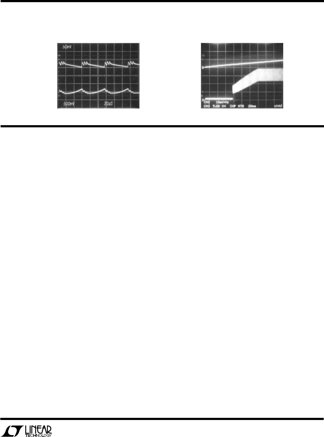
Soft Start: Load Current vs Time
Burst Mode Operation
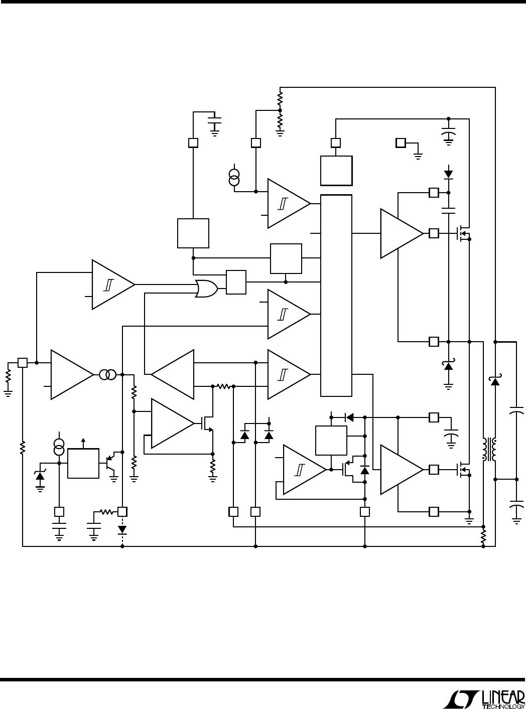
PIN FUNCTIONS
UUU
ever EXTV
CC
is higher than 4.7V. See EXTV
CC
connection
in Applications Information section. Do not exceed 10V on
this pin. Connect to V
OUT
if V
OUT
≥ 5V.
PGND (Pin 10): Driver Power Ground. Connects to source
of bottom N-channel MOSFET and the (–) terminal of C
IN
.
BG (Pin 11): High Current Gate Drive for Bottom
N-Channel MOSFET. Voltage swing at this pin is from
ground to INTV
CC
.
INTV
CC
(Pin 12): Output of the Internal 5V Regulator and
EXTV
CC
Switch. The driver and control circuits are pow-
ered from this voltage. Must be closely decoupled to power
ground with a minimum of 2.2µF tantalum or electrolytic
capacitor.
V
IN
(Pin 13): Main Supply Pin. Must be closely decoupled
to the IC’s signal ground pin.
SW (Pin 14): Switch Node Connection to Inductor. Volt-
age swing at this pin is from a Schottky diode (external)
voltage drop below ground to V
IN
.
BOOST (Pin 15): Supply to Topside Floating Driver. The
bootstrap capacitor is returned to this pin. Voltage swing
at this pin is from INTV
CC
to V
IN
+ INTV
CC
.
TG (Pin 16): High Current Gate Drive for Top N-Channel
MOSFET. This is the output of a floating driver with a
voltage swing equal to INTV
CC
superimposed on the
switch node voltage SW.
C
OSC
(Pin 1): External capacitor C
OSC
from this pin to
ground sets the operating frequency.
RUN/SS (Pin 2): Combination of Soft Start and Run
Control Inputs. A capacitor to ground at this pin sets the
ramp time to full current output. The time is approximately
0.5s/µF. Forcing this pin below 1.3V causes the device to
be shut down. In shutdown all functions are disabled.
I
TH
(Pin 3): Error Amplifier Compensation Point. The
current comparator threshold increases with this control
voltage. Nominal voltage range for this pin is 0V to 2.5V.
SFB (Pin 4): Secondary Winding Feedback Input. Nor-
mally connected to a feedback resistive divider from the
secondary winding. This pin should be tied to: ground to
force continuous operation; INTV
CC
in applications that
don’t use a secondary winding; and a resistive divider from
the output in applications using a secondary winding.
SGND (Pin 5): Small-Signal Ground. Must be routed
separately from other grounds to the (–) terminal of C
OUT
.
V
OSENSE
(Pin 6): Receives the feedback voltage from an
external resistive divider across the output.
SENSE
–
(Pin 7): The (–) Input to the Current Comparator.
SENSE
+
(Pin 8): The (+) Input to the Current Comparator.
Built-in offsets between SENSE
–
and SENSE
+
pins in
conjunction with R
SENSE
set the current trip thresholds.
EXTV
CC
(Pin 9): Input to the Internal Switch Connected to
INTV
CC
. This switch closes and supplies V
CC
power when-
I
LOAD
= 50mA 1435 G16
V
OUT
20mV/DIV
V
ITH
200mV/DIV
1435 G17
RUN/SS
5V/DIV
INDUCTOR
CURRENT
1A/DIV