10
LTC1435
APPLICATIONS INFORMATION
WUU
U
where δ is the temperature dependency of R
DS(ON)
and k
is a constant inversely related to the gate drive current.
Both MOSFETs have I
2
R losses while the topside
N-channel equation includes an additional term for tran-
sition losses, which are highest at high input voltages.
For V
IN
< 20V the high current efficiency generally im-
proves with larger MOSFETs, while for V
IN
> 20V the
transition losses rapidly increase to the point that the use
of a higher R
DS(ON)
device with lower C
RSS
actual pro-
vides higher efficiency. The synchronous MOSFET losses
are greatest at high input voltage or during a short circuit
when the duty cycle in this switch is nearly 100%. Refer
to the Foldback Current Limiting section for further
applications information.
The term (1 + δ) is generally given for a MOSFET in the
form of a normalized R
DS(ON)
vs Temperature curve, but
δ = 0.005/°C can be used as an approximation for low
voltage MOSFETs. C
RSS
is usually specified in the MOSFET
characteristics. The constant k = 2.5 can be used to
estimate the contributions of the two terms in the main
switch dissipation equation.
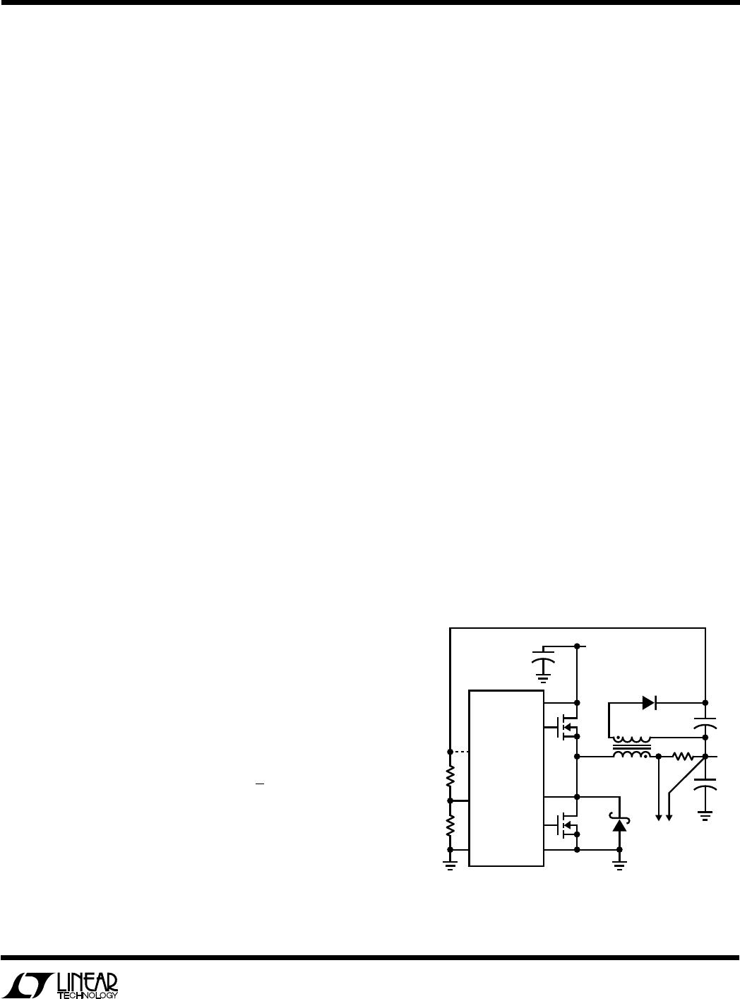
The Schottky diode D1 shown in Figure 1 conducts during
the dead-time between the conduction of the two large
power MOSFETs. This prevents the body diode of the
bottom MOSFET from turning on and storing charge
during the dead-time, which could cost as much as 1% in
efficiency. A 1A Schottky is generally a good size for 3A
regulators.
C
IN
and C
OUT
Selection
In continuous mode, the source current of the top
N-channel MOSFET is a square wave of duty cycle V
OUT
/
V
IN
. To prevent large voltage transients, a low ESR input
capacitor sized for the maximum RMS current must be
used. The maximum RMS capacitor current is given by:
C required
IN
II
VVV
V
RMS MAX
OUT IN OUT
IN
()
[]
12/
This formula has a maximum at V
IN
= 2V
OUT
, where
I
RMS
= I
OUT
/2. This simple worst-case condition is com-
monly used for design because even significant deviations
do not offer much relief. Note that capacitor manufacturer’s
ripple current ratings are often based on only 2000 hours
of life. This makes it advisable to further derate the
capacitor or to choose a capacitor rated at a higher
temperature than required. Several capacitors may also be
paralleled to meet size or height requirements in the
design. Always consult the manufacturer if there is any
question.
The selection of C
OUT
is driven by the required effective
series resistance (ESR). Typically, once the ESR require-
ment is satisfied the capacitance is adequate for filtering.
The output ripple (V
OUT
) is approximated by:
∆∆V I ESR
fC
OUT L
OUT
≈+
1
4
where f = operating frequency, C
OUT
= output capacitance
and I
L
= ripple current in the inductor. The output ripple
is highest at maximum input voltage since I
L
increases
with input voltage. With I
L
= 0.4I
OUT(MAX)
the output
ripple will be less than 100mV at max V
IN
assuming:
C
OUT
required ESR < 2R
SENSE
Manufacturers such as Nichicon, United Chemicon and
Sanyo should be considered for high performance through-
hole capacitors. The OS-CON semiconductor dielectric
capacitor available from Sanyo has the lowest ESR(size)
product of any aluminum electrolytic at a somewhat
higher price. Once the ESR requirement for C
OUT
has been
met, the RMS current rating generally far exceeds the
I
RIPPLE(P-P)
requirement.
In surface mount applications multiple capacitors may
have to be paralleled to meet the ESR or RMS current
handling requirements of the application. Aluminum elec-
trolytic and dry tantalum capacitors are both available in
surface mount configurations. In the case of tantalum, it is
critical that the capacitors are surge tested for use in
switching power supplies. An excellent choice is the AVX
TPS series of surface mount tantalum, available in case
heights ranging from 2mm to 4mm. Other capacitor types
include Sanyo OS-CON, Nichicon PL series and Sprague
593D and 595D series. Consult the manufacturer for other
specific recommendations.
11
LTC1435
additional circuitry is required to derive INTV
CC
power
from the output.
The following list summarizes the four possible connec-
tions for EXTV
CC:
1. EXTV
CC
left open (or grounded). This will cause INTV
CC
to be powered from the internal 5V regulator resulting
in an efficiency penalty of up to 10% at high input
voltages.
2. EXTV
CC
connected directly to V
OUT
. This is the normal
connection for a 5V regulator and provides the highest
efficiency.
3. EXTV
CC
connected to an output-derived boost network.
For 3.3V and other low voltage regulators, efficiency
gains can still be realized by connecting EXTV
CC
to an
output-derived voltage which has been boosted to
greater than 4.8V. This can be done with either the
inductive boost winding as shown in Figure 4a or the
capacitive charge pump shown in Figure 4b. The charge
pump has the advantage of simple magnetics.
4. EXTV
CC
connected to an external supply. If an external
supply is available in the 5V to 10V range (EXTV
CC
V
IN
), it may be used to power EXTV
CC
providing it is
compatible with the MOSFET gate drive requirements.
When driving standard threshold MOSFETs, the exter-
nal supply must always be present during operation to
prevent MOSFET failure due to insufficient gate drive.
APPLICATIONS INFORMATION
WUU
U
INTV
CC
Regulator
An internal P-channel low dropout regulator produces the
5V supply which powers the drivers and internal circuitry
within the LTC1435. The INTV
CC
pin can supply up to
15mA and must be bypassed to ground with a minimum
of 2.2µF tantalum or low ESR electrolytic. Good bypassing
is necessary to supply the high transient currents required
by the MOSFET gate drivers.
High input voltage applications, in which large MOSFETs
are being driven at high frequencies, may cause the
maximum junction temperature rating for the LTC1435 to
be exceeded. The IC supply current is dominated by the
gate charge supply current when not using an output
derived EXTV
CC
source. The gate charge is dependent on
operating frequency as discussed in the Efficiency Consid-
erations section. The junction temperature can be esti-
mated by using the equations given in Note 1 of the
Electrical Characteristics. For example, the LTC1435 is
limited to less than 17mA from a 30V supply:
T
J
= 70°C + (17mA)(30V)(100°C/W) = 126°C
To prevent maximum junction temperature from being
exceeded, the input supply current must be checked when
operating in continuous mode at maximum V
IN
.
EXTV
CC
Connection
The LTC1435 contains an internal P-channel MOSFET
switch connected between the EXTV
CC
and INTV
CC
pins.
The switch closes and supplies the INTV
CC
power when-
ever the EXTV
CC
pin is above 4.8V, and remains closed
until EXTV
CC
drops below 4.5V. This allows the MOSFET
driver and control power to be derived from the output
during normal operation (4.8V < V
OUT
< 9V) and from the
internal regulator when the output is out of regulation
(start-up, short circuit). Do not apply greater than 10V to
the EXTV
CC
pin and ensure that EXTV
CC
< V
IN
.
Significant efficiency gains can be realized by powering
INTV
CC
from the output, since the V
IN
current resulting
from the driver and control currents will be scaled by a
factor of Duty Cycle/Efficiency. For 5V regulators this
supply means connecting the EXTV
CC
pin directly to V
OUT
.
However, for 3.3V and other lower voltage regulators,
Figure 4a. Secondary Output Loop and EXTV
CC
Connection
R6
R5
EXTV
CC
SFB
SGND
V
IN
TG
BG
PGND
LTC1435
N-CH
N-CH
+
C
IN
V
IN
1N4148
+
1µF
+
C
OUT
V
SEC
L1
1:N
R
SENSE
V
OUT
OPTIONAL
EXT V
CC
CONNECTION
5V V
SEC
9V
LTC1435 • F04a
SW
12
LTC1435
APPLICATIONS INFORMATION
WUU
U
EXTV
CC
V
IN
TG
BG
PGND
LTC1435
N-CH
N-CH
+
C
IN
V
IN
+
C
OUT
L1
R
SENSE
V
OUT
+
1µF
LTC1435 • F04b
VN2222LL
BAT85 BAT85
BAT85
0.22µF
SW
Figure 4b. Capacitive Charge Pump for EXTV
CC
Topside MOSFET Driver Supply (C
B
, D
B
)
An external bootstrap capacitor C
B
connected to the Boost
pin supplies the gate drive voltage for the topside MOSFET.
Capacitor C
B
in the Functional Diagram is charged through
diode D
B
from INTV
CC
when the SW pin is low. When the
topside MOSFET is to be turned on, the driver places the
C
B
voltage across the gate source of the MOSFET. This
enhances the MOSFET and turns on the topside switch.
The switch node voltage SW rises to V
IN
and the Boost pin
rises to V
IN
+ INTV
CC
. The value of the boost capacitor C
B
needs to be 100 times greater than the total input capaci-
tance of the topside MOSFET. In most applications 0.1µF
is adequate. The reverse breakdown on D
B
must be greater
than V
IN(MAX).
Output Voltage Programming
The output voltage is set by a resistive divider according
to the following formula:
VV
R
R
OUT
=+
119 1
2
1
.
The external resistor divider is connected to the output as
shown in Figure 5 allowing remote voltage sensing.
Run/Soft Start Function
The RUN/SS pin is a dual purpose pin which provides the
soft start function and a means to shut down the LTC1435.
Figure 6. RUN/SS Pin Interfacing
Soft start reduces surge currents from V
IN
by gradually
increasing the internal current limit.
Power supply se-
quencing
can also be accomplished using this pin.
An internal 3µA current source charges up an external
capacitor C
SS.
When the voltage on RUN/SS reaches 1.3V
the LTC1435 begins operating. As the voltage on RUN/SS
continues to ramp from 1.3V to 2.4V, the internal current
limit is also ramped at a proportional linear rate. The
current limit begins at approximately 50mV/R
SENSE
(at
V
RUN/SS
= 1.3V) and ends at 150mV/R
SENSE
(V
RUN/SS
>
2.7V). The output current thus ramps up slowly, charging
the output capacitor. If RUN/SS has been pulled all the way
to ground there is a delay before starting of approximately
500ms/µF, followed by an additional 500ms/µF to reach
full current.
t
DELAY
= 5(10
5
)C
SS
Seconds
Pulling the RUN/SS pin below 1.3V puts the LTC1435 into
a low quiescent current shutdown (I
Q
< 25µA). This pin
can be driven directly from logic as shown in Figure 6.
Diode D1 in Figure 6 reduces the start delay but allows
C
SS
to ramp up slowly for the soft start function; this
diode and C
SS
can be deleted if soft start is not needed.
The RUN/SS pin has an internal 6V Zener clamp (See
Functional Diagram).
V
OSENSE
LTC1435
R1
R2
LTC1435 • F05
100pF
1.19V V
OUT
9V
SGND
Figure 5. Setting the LTC1435 Output Voltage

LTC1435IG#PBF

Mfr. #:
Manufacturer:
Analog Devices / Linear Technology
Description:
Switching Voltage Regulators See P/N LTC1435AIG for Upgrade/
Lifecycle:
New from this manufacturer.
Delivery:
DHL FedEx Ups TNT EMS
Payment:
T/T Paypal Visa MoneyGram Western Union