AD734
Rev. E | Page 12 of 20
This error is not important in some closed-loop applications,
such as automatic gain control (AGC), but clearly is not acceptable
where the denominator value must be well-defined. When it is
required to set up an accurate, fixed value of U, the on-chip
reference can be used. The transistor Qr is provided to cancel
the V
BE
of Qu, and is biased by an external resistor, R2, as shown
in Figure 23. R1 is chosen to set the desired value of U and
consists of a fixed and adjustable resistor.
4
14
9
13
8
U0
Iu
Qu
NC
Qr
Ru
28k
Rr
100k
VP
VN
DD
ER
NC
+V
S
~60µA
–V
S
U1
U2
AD734
00827-005
V
G
+
3
5
Figure 22. Low Accuracy Denominator Control
4
14
9
13
8
U0
Iu
Qu
NC
Qr
Ru
28k
Rr
100k
VP
VN
DD
R2
ER
+V
S
–V
S
U1
U2
AD734
00827-006
3
5
R1
NOM
8V
Figure 23. Connections for a Fixed Denominator
Table 5 shows useful values of the external components for
setting up nonstandard denominator values.
Table 5. Component Values for Setting Up Nonstandard
Denominator Values
Denominator R1 (Fixed) R1 (Variable) R2
5 V 34.8 kΩ 20 kΩ 120 kΩ
3 V 64.9 kΩ 20 kΩ 220 kΩ
2 V 86.6 kΩ 50 kΩ 300 kΩ
1 V 174 kΩ 100 kΩ 620 kΩ
The denominator can also be current controlled, by grounding
Pin 3 (U0) and withdrawing a current of Iu from Pin 4 (U1).
The nominal scaling relationship is U = 28 × Iu, where u is
expressed in volts and Iu is expressed in milliamps. Note,
however, that while the linearity of this relationship is very
good, it is subject to a scale tolerance of ±20%. Note that the
common-mode range on Pin 3 through Pin 5 actually extends
from 4 V to 36 V below VP; therefore, it is not necessary to
restrict the connection of U0 to ground to use some other
voltage.
The output ER can also be buffered, rescaled, and used as a
general-purpose reference voltage. It is generated with respect
to the negative supply line, Pin 8 (VN), but this is acceptable
when driving one of the signal interfaces. An example is shown
in Figure 31, where a fixed numerator of 10 V is generated for a
divider application. Y2 is tied to VN, but Y1 is 10 V above this;
therefore, the common-mode voltage at this interface is still 5 V
above VN, which satisfies the internal biasing requirements (see
Table 1).
OPERATION AS A MULTIPLIER
All of the connection schemes used in this section are essentially
identical to those used for the AD534, with which the AD734 is
pin compatible. The only precaution to be noted in this regard
is that in the AD534, Pin 3, Pin 5, Pin 9, and Pin 13 are not
internally connected, and Pin 4 has a slightly different purpose.
In many cases, an AD734 can be directly substituted for an
AD534 with immediate benefits in static accuracy, distortion,
feedthrough, and speed. Where Pin 4 was used in an AD534
application to achieve a reduced denominator voltage, this
function can now be much more precisely implemented with
the AD734 using alternative connections (see the Direct
Denominator Control section).
Operation from supplies down to ±8 V is possible. The supply
current is essentially independent of voltage. As is true of all
high speed circuits, careful power supply decoupling is important
in maintaining stability under all conditions of use. The decoupling
capacitors should always be connected to the load ground,
because the load current circulates in these capacitors at high
frequencies. Note the use of the special symbol (a triangle with
the letter L inside it) to denote the load ground (see Figure 24).
Standard Multiplier Connections
Figure 24 shows the basic connections for multiplication. The X
and Y inputs are shown as optionally having their negative nodes
grounded, but they are fully differential, and in many applications
the grounded inputs can be reversed (to facilitate interfacing
with signals of a particular polarity, while achieving some desired
output polarity) or both can be driven.
The AD734 has an input resistance of 50 kΩ ± 20% at the X, Y,
and Z interfaces, which allows ac coupling to be achieved with
moderately good control of the high-pass (HP) corner frequency;
a capacitor of 0.1 μF provides a HP corner frequency of 32 Hz.
When a tighter control of this frequency is needed, or when the
HP corner is above about 100 kHz, an external resistor should
be added across the pair of input nodes.
AD734
X11
X22
U0
3
U1
4
U2
5
VP 14
DD
NC
NC
13
W
12
Z1
11
Z2
10
Y27
ER 9
VN 8
Y16
L
L
X
INPUT
±10V FS
Y INPUT
±10V FS
+15V
Z
2
–15V
0.1µF
0.1µF
LOAD
GROUND
OPTIONAL
SUMMING INPUT
±10V FS
W =
+ Z
2
(X
1
– X
2
)(Y
1
–Y
2
)
10V
00827-007
Figure 24. Basic Multiplier Circuit
AD734
Rev. E | Page 13 of 20
At least one of the two inputs of any pair must be provided with
a dc path (usually to ground). The careful selection of ground
returns is important in realizing the full accuracy of the AD734.
The Z2 pin is normally connected to the load ground, which can be
remote in some cases. It can also be used as an optional summing
input (see Equation 3 and Equation 4) having a nominal FS
input of ±10 V and the full 10 MHz bandwidth.
In applications where high absolute accuracy is essential, the
scaling error caused by the finite resistance of the signal source(s)
may be troublesome; for example, a 50 Ω source resistance at
just one input introduces a gain error of −0.1%; if both the X
and Y inputs are driven from 50 Ω sources, the scaling error in
the product is −0.2%. If the source resistances are known, this
gain error can be completely compensated by including the
appropriate resistance (50 Ω or 100 Ω, respectively, in the
preceding cases) between the output, W (Pin 12), and the Z1
feedback input (Pin 11). If Rx is the total source resistance
associated with the X1 and X2 inputs, and Ry is the total source
resistance associated with the Y1 and Y2 inputs, and neither Rx
nor Ry exceeds 1 kΩ, a resistance of Rx + Ry in series with
Pin Z1 provides the required gain restoration.
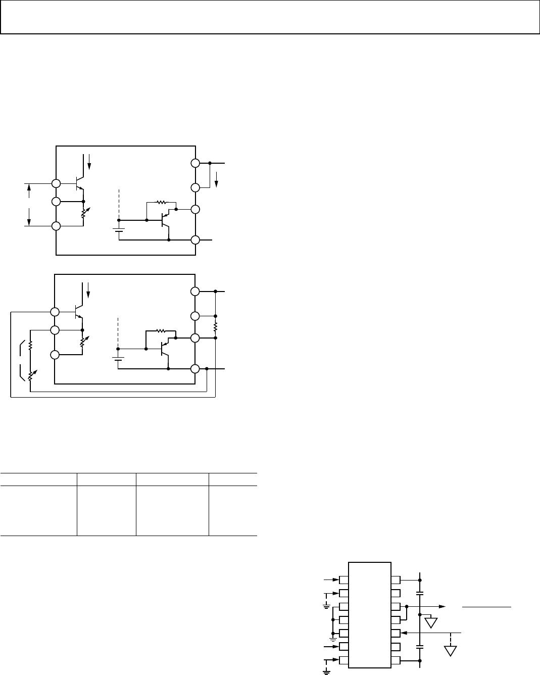
Pin 9 (ER) and Pin 13 (DD) should be left unconnected in this
application. The U inputs (Pin 3, Pin 4, and Pin 5) are shown
connected to ground; they can alternatively be connected to
VN, if desired. In applications where Pin 2 (X2) happens to
be driven with a high amplitude, high frequency signal, the
capacitive coupling to the denominator control circuitry via
an ungrounded Pin 3 can cause high frequency distortion.
However, the AD734 can be operated without modification in
an
AD534 socket and these three pins left unconnected with the
preceding caution noted.
AD734
X1
1
X2
2
U0
3
U1
4
U2
5
VP
14
DD
NC
NC
13
W
12
Z1
11
Z2
10
Y2
7
ER
9
VN
8
Y1
6
L
L
X INPUT
±10V FS
Y INPUT
±10V FS
+15
R
S
–15V
0.1µF
0.1µF
L
LOAD
±10mA MAX FS
±10V MAXIMUM
LOAD VOLTAGE
I
W
I
W
=
(X
1
– X
2
)(Y
1
–Y
2
)
10V
+
1
R
S
1
50k
0
0827-008
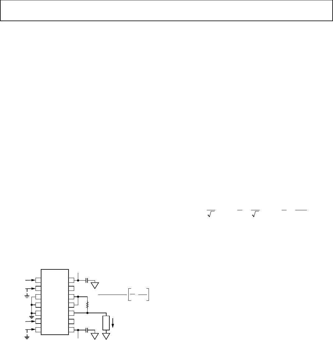
Figure 25. Conversion of Output to a Current
Current Output
It may occasionally be desirable to convert the output voltage to
a current. In correlation applications, for example, multiplication is
followed by integration; if the output is in the form of a current,
a simple grounded capacitor can perform this function. Figure 25
shows how this can be achieved. The op amp forces the voltage
across Z1 and Z2, and thus across the resistor, RS, to be the
product XY/U. Note that the input resistance of the Z interface
is in shunt with RS, which must be calculated accordingly.
The smallest FS current is simply ±10 V/50 kΩ, or ±200 μA,
with a tolerance of about 20%. To guarantee a 1% conversion
tolerance without adjustment, R
S
must be less than 2.5 kΩ. The
maximum full-scale output current should be limited to about
±10 mA (thus, R
S
= 1 kΩ). This concept can be applied to all
connection modes, with the appropriate choice of terminals.
Squaring and Frequency-Doubling
Squaring of an input signal, E, is achieved by connecting the X
and Y inputs in parallel; the phasing can be chosen to produce
an output of E
2
/U or −E
2
/U as desired. The input can have
either polarity, but the basic output is either always positive or
negative; as for multiplication, the Z2 input can be used to add a
further signal to the output.
When the input is a sine wave, a squarer behaves as a frequency
doubler, because
(Esinwt)
2
= E
2
(1 − cos2wt)/2 (8)
Equation 8 shows a dc term at the output, which varies strongly
with the amplitude of the input, E. This dc term can be avoided
using the connection shown in Figure 26, where an RC network
is used to generate two signals whose product has no dc term.
The output is
+=
V10
1
4
sin
2
4
sin
2
4
ππ
wt
E
wt
E
W
(9)
for w = 1/CR1, which is just
W = E
2
(cos2wt)/(10 V) (10)
which has no dc component. To restore the output to ±10 V
when E = 10 V, a feedback attenuator with an approximate ratio
of 4 is used between W and Z1; this technique can be used
wherever it is desired to achieve a higher overall gain in the
transfer function.
The values of R3 and R4 include additional compensation for the
effects of the 50 kΩ input resistance of all three interfaces; R2 is
included for a similar reason. These resistor values should not
be altered without careful calculation of the consequences. With
the values shown, the center frequency f
0
is 100 kHz for C =
1 nF. The amplitude of the output is only a weak function of
frequency; the output amplitude is 0.5% too low at f = 0.9f
0
and
f = 1.1f
0
. The cross-connection is simply to produce the cosine
output with the sign shown in Equation 10; however, the sign in
this case is rarely important.
AD734
Rev. E | Page 14 of 20
AD734
X1
1
X2
2
U0
3
U1
4
U2
5
VP
14
DD
NC
C
NC
13
W
12
Z1
11
Z2
10
Y2
7
ER
9
VN
8
Y1
6
L
L
L
+15
R4
4.32k
R3
13k
R1
1.6k
R2
1.6k
–15V
0.1µF
0.1µF
0
0827-009
Esinωt E
2
cos2ωt/10V
Figure 26. Frequency Doubler
OPERATION AS A DIVIDER
The AD734 supports two methods for performing analog
division. The first is based on the use of a multiplier in a
feedback loop. This is the standard mode recommended for
multipliers having a fixed scaling voltage, such as the AD534,
and is described in this section. The second uses the AD734’s
unique capability for externally varying the scaling (denominator)
voltage directly, and is described in the Division by Direct
Denominator Control section.
Feedback Divider Connections
Figure 27 shows the connections for the standard (AD534)
divider mode. Feedback from the output, W, is now taken to the
Y2 (inverting) input, which, if the X input is positive, establishes a
negative feedback path. Y1 should normally be connected to the
ground associated with the load circuit, but can optionally be
used to sum a further signal to the output. If desired, the
polarity of the Y input connections can be reversed, with W
connected to Y1 and Y2 used as the optional summation input. In
this case, either the polarity of the X input connections must be
reversed or the X input voltage must be negative.
AD734
X1
1
X2
2
U0
3
U1
4
U2
5
VP
14
DD
NC
NC
13
W
12
Z1
11
Z2
10
Y2
7
ER
9
VN
8
Y1
6
L
L
X INPUT
+0.1V TO
+10V
Y
1
OPTIONAL
SUMMING
INPUT
±10V FS
+15
Z INPUT
±10V FS
–15V
0.1µF
0.1µF
W = 10 +Y1
(Z
2
– Z
1
)
(X
1
– X
2
)
00827-010
L
Figure 27. Standard (AD534) Divider Connection
The numerator input, which is differential and can have either
polarity, is applied to Pin Z1 and Pin Z2. As with all dividers
based on feedback, the bandwidth is directly proportional to
the denominator, being 10 MHz for X = 10 V and reducing to
100 kHz for X = 100 mV. This reduction in bandwidth, and
the increase in output noise (which is inversely proportional
to the denominator voltage) preclude operation much below a
denominator of 100 mV. Division using direct control of the
denominator (see Figure 29) does not have these shortcomings.
AD734
X1
1
X2
2
U0
3
U1
4
U2
5
VP
14
DD
NC
NC
13
W
12
Z1
11
Z2
10
Y2
7
ER
9
VN
8
Y1
6
L
L
S
OPTIONAL
SUMMING
INPUT
±10V FS
+15
V
Z INPUT
+10mV TO
+10V
–15V
0.1µF
0.1µF
00827-011
L
D
+
W = (10V) (Z
2
– Z
1
) + S
Figure 28. Connection for Square Rooting
Connections for Square-Rooting
The AD734 can be used to generate an output proportional to
the square root of an input using the connections shown in
Figure 28. Feedback is now via both the X and Y inputs, and is
always negative because of the reversed polarity between these
two inputs. The Z input must have the polarity shown, but
because it is applied to a differential port, either polarity of
input can be accepted with reversal of Z1 and Z2, if necessary.
The diode, D, which can be any small-signal type (1N4148
being suitable), is included to prevent a latching condition,
which can occur if the input is momentarily of the incorrect
polarity of the input. The output is always negative.
Note that the loading on the output side of the diode is provided
by the 25 kΩ of input resistance at X1 and Y2, and by the user’s
load. In high speed applications, it may be beneficial to include
further loading at the output (to 1 kΩ minimum) to speed up
response time. As in previous applications, a further signal, shown
in Figure 28 as S, can be summed to the output; if this option is
not used, this node should be connected to the load ground.
DIVISION BY DIRECT DENOMINATOR CONTROL
The AD734 can be used as an analog divider by directly varying
the denominator voltage. In addition to providing much higher
accuracy and bandwidth, this mode also provides greater
flexibility, because all inputs remain available. Figure 29 shows
the connections for the general case of a three-input multiplier
divider, providing the function
2
21
2121
)(
))((
Z
UU
YYXX
W +
= (11)
where the
X, Y, and Z signals can all be positive or negative,
but the difference U = U
1
− U
2
must be positive and in the range
10 mV to 10 V. If a negative denominator voltage must be used,
simply ground the noninverting input of the op amp. As previ-
ously noted, the X input must have a magnitude of less than 1.25U.

AD734ANZ

Mfr. #:
Manufacturer:
Description:
Multipliers / Dividers 10MHz 4-Quadrant
Lifecycle:
New from this manufacturer.
Delivery:
DHL FedEx Ups TNT EMS
Payment:
T/T Paypal Visa MoneyGram Western Union