AD734
Rev. E | Page 15 of 20
AD734
X1
1
X2
2
U0
3
U1
4
U2
U
1
2M
U
2
5
VP
14
DD
NC
13
W
12
Z1
11
Z2
10
Y2
7
ER
9
VN
8
Y1
6
L
Z
2
OPTIONAL
SUMMING
INPUT
±10V FS
+15V
–15V
0.1µF
0.1µF
00827-012
X INPUT
Y INPUT
LOAD
GROUND
L
W =
+ Z
2
(X
1
– X
2
)(Y
1
–Y
2
)
U
1
– U
2
U INPUT
Figure 29. Three-Variable Multiplier/Divider Using Direct Denominator
Control
This connection scheme can also be viewed as a variable-gain
element, whose output, in response to a signal at the X input, is
controllable by both the Y input (for attenuation, using Y less
than U) and the U input (for amplification, using U less than
Y). The ac performance is shown in Figure 30; for these results,
Y was maintained at a constant 10 V. At U = 10 V, the gain is
unity and the circuit bandwidth is a full 10 MHz. At U = 1 V,
the gain is 20 dB and the bandwidth is essentially unaltered. At
U = 100 mV, the gain is 40 dB and the bandwidth is 2 MHz.
Finally, at U = 10 mV, the gain is 60 dB and the bandwidth is
250 kHz, corresponding to a 250 MHz gain-bandwidth product.
FREQUENCY (Hz)
GAIN (IdB)
70
60
50
40
30
20
10
0
10k 100k 1M 10M
00827-013
U = 10mV
U = 10V
U = 100mV
U
=
1
V
Figure 30. Three-Variable Multiplier/Divider Performance
The 2 MΩ resistor is included to improve the accuracy of the
gain for small denominator voltages. At high gains, the X input
offset voltage can cause a significant output offset voltage. To
eliminate this problem, a low-pass feedback path can be used
from W to X2; see Figure 32 for details.
Where a numerator of 10 V is needed, to implement a two-
quadrant divider with fixed scaling, the connections shown in
Figure 31 can be used. The reference voltage output appearing
between Pin 9 (ER) and Pin 8 (VN) is amplified and buffered by
the second op amp, to impose 10 V across the Y1/Y2 input.
Note that Y2 is connected to the negative supply in this application.
This is permissible because the common-mode voltage is still
high enough to meet the internal requirements.
The transfer function is
2
21
21
10 Z
UU
XX
VW +
= (12)
The ac performance of this circuit remains as shown in Figure 30.
AD734
X1
1
X2
2
U0
3
U1
4
U2
U
1
U
2
5
VP
14
DD
13
W
12
Z1
11
Z2
10
Y2
7
ER
9
VN
8
Y1
6
L
Z
2
OPTIONAL
SUMMING
INPUT
±10V FS
+15
V
–15V
0.1µF
0.1µF
00827-014
X INPUT
2M
LOAD
GROUND
L
W =
+ Z
2
(X
1
– X
2
)10V
U
1
– U
2
U INPUT
200k
100k
SCALE
AJDUST
OP AMP = AD712 DUAL
Figure 31. Two-Quadrant Divider with Fixed 10 V Scaling
A PRECISION AGC LOOP
The variable denominator of the AD734 and its high gain
bandwidth product make it an excellent choice for precise
automatic gain control (AGC) applications. Figure 32 shows a
suggested method. The input signal, E
IN
, which can have a peak
amplitude from 10 mV to 10 V at any frequency from 100 Hz to
10 MHz, is applied to the X input and a fixed positive voltage E
C
to the Y input. Op Amp A2 and Capacitor C2 form an integrator
with a current summing node at its inverting input. (The AD712
dual op amp is a suitable choice for this application.) In the absence
of an input, the current in D2 and R2 causes the integrator output
to ramp negative, clamped by Diode D3, which is included to
reduce the time required for the loop to establish a stable,
calibrated, output level after the circuit has received an input
signal. With no input to the denominator (U0 and U2), the gain
of the AD734 is very high (about 70 dB), and thus even a small
input causes a substantial output.
AD734
X11
X2
2
U03
U1
4
U25
VP 14
DD
13
W 12
Z1
11
Z2 10
Y2
7
ER 9
VN
8
Y16
L
L
+15V
–15V
00827-015
OP AMP = AD712 DUA L
A1
A2
C1
1µF
C1
1µF
C2
1µF
E
IN
E
C
+
1
V
TO
+10V
D3
1N914
D1
1N914
D2
1N914
R2
1M
R1
1M
R3
1M
NC
E
OUT
0.1µF
0.1µF
Figure 32. Precision AGC Loop
Diode D1 and C1 form a peak detector, which rectifies the output
and causes the integrator to ramp positive. When the current in
R1 balances the current in R2, the integrator output holds the
denominator output at a constant value. This occurs when there
AD734
Rev. E | Page 16 of 20
is sufficient gain to raise the amplitude of E
IN
to that required to
establish an output amplitude of E
C
over the range of 1 V to 10 V.
The X input of the AD734, which has finite offset voltage, can be
troublesome at the output at high gains. The output offset is
reduced to that of the X input (1 mV or 2 mV) by the offset
loop comprising R3, C3, and Buffer A1. The low-pass corner
frequency of 0.16 Hz is transformed to a high-pass corner that is
multiplied by the gain (for example, 160 Hz at a gain of 1000).
In applications not requiring operation down to low frequencies,
Amplifier A1 can be eliminated, but the AD734’s input resistance
of 50 kΩ between X1 and X2 reduces the time constant and
increases the input offset. Using a nonpolar 20 mF tantalum
capacitor for C1 results in the same unity-gain high-pass corner; in
this case, the offset gain increases to 20, which is still acceptable.
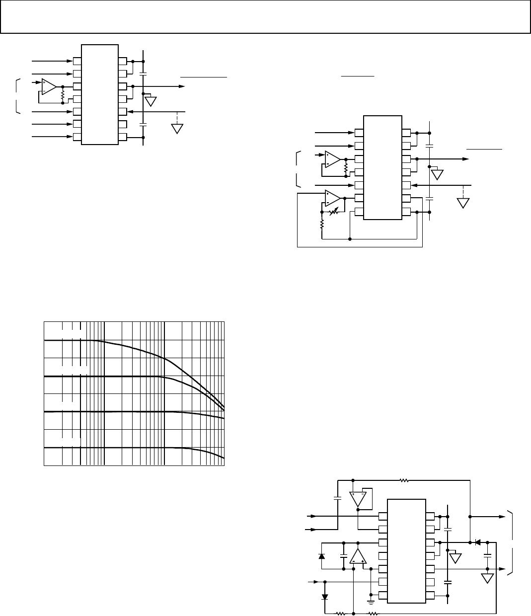
Figure 33 shows the error in the output for sinusoidal inputs at
100 Hz, 100 kHz, and 1 MHz, with E
C
set to 10 V. The output
error for any frequency between 300 Hz and 300 kHz is similar
to that for 100 kHz. At low signal frequencies and low input
amplitudes, the dynamics of the control loop determine the gain
error and distortion; at high frequencies, the 200 MHz gain-
bandwidth product of the AD734 limits the available gain.
The output amplitude tracks E
C
over the range of 1 V to slightly
more than 10 V.
INPUT AMPLITUDE (V)
ERROR (dB)
2
1
0
–1
–2
0.01 0.1 1 10
00827-016
100kHz
100Hz
1MHz
Figure 33. AGC Amplifier Output Error vs. Input Voltage
WIDEBAND RMS-TO-DC CONVERTER USING U
INTERFACE
The AD734 is well-suited to such applications as implicit rms-
to-dc conversion, where the AD734 implements the function
[]
RMS
IN
RMS
V
V
V
2
avg
= (13)
using its direct divide mode. Figure 34 shows the circuit.
AD734
X11
X22
U03
U14
U2
5
VP 14
DD 13
W 12
Z1 11
Z2
10
Y2
7
ER
9
VN
8
Y16
+15
U2b
1/2
AD708
1/2
AD708
–15V
0.1µF
0.1µF
00827-017
L
L
L
L
L
C1
47µF
C2
1µF
V
IN
R1
3.32k
U2a
L
L
V
O
= V
IN
2
Figure 34. A Two-Chip, Wideband RMS-to-DC Converter
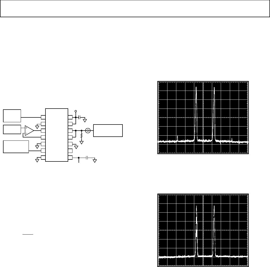
In this application, the AD734 and an AD708 dual op amp
serve as a two-chip rms-to-dc converter with a 10 MHz
bandwidth. Figure 35 shows the circuits performance for
square-, sine-, and triangle-wave inputs. The circuit accepts
signals as high as 10 V p-p with a crest factor of 1 or 1 V p-p
with a crest factor of 10. The circuits response is flat to 10 MHz
with an input of 10 V, flat to almost 5 MHz for an input of 1 V,
and to almost 1 MHz for inputs of 100 mV. For accurate
measurements of input levels below 100 mV, the AD734’s
output offset (Z interface) voltage, which contributes a dc error,
must be trimmed out.
In the circuit shown in Figure 34, the AD734 squares the input
signal, and its output (V
IN
2
) is averaged by a low-pass filter that
consists of R1 and C1 and has a corner frequency of 1 Hz. Because
of the implicit feedback loop, this value is both the output value,
V
RMS
, and the denominator in Equation 13. U2a and U2b, an
AD708 dual dc precision op amp, serve as unity-gain buffers,
supplying both the output voltage and driving the U interface.
INPUT FREQUENCY (Hz)
OUTPUT VOLTAGE (V)
100
10
1
100m
1m
10m
100µ
10k 100k 1M 10M
00827-018
SQUARE WAVE
SINE WAVE
TRI-WAVE
Figure 35. RMS-to-DC Converter Performance
AD734
Rev. E | Page 17 of 20
The possible two-tone intermodulation products are at 2 ×
9.95 MHz − 10.05 MHz ± 9.00 MHz and 2 × 10.05 − 9.95 MHz
± 9.00 MHz; of these, only the third-order products at 0.850 MHz
and 1.150 MHz are within the 10 MHz bandwidth of the AD734;
the desired output signals are at 0.950 MHz and 1.050 MHz.
Note that the difference between the desired outputs and third-
order products (see Figure 37) is approximately 78 dB, which
corresponds to a computed third-order intercept point of +46 dBm.
LOW DISTORTION MIXER
The AD734’s low noise and distortion make it especially suitable
for use as a mixer, modulator, or demodulator. Although the
AD734’s −3 dB bandwidth is typically 10 MHz and is established
by the output amplifier, the bandwidth of its X and Y interfaces
and the multiplier core are typically in excess of 40 MHz. Thus,
provided that the desired output signal is less than 10 MHz, as
is typically the case in demodulation, the AD734 can be used
with both its X and Y input signals as high as 40 MHz. One test
of mixer performance is to linearly combine two closely spaced,
equal-amplitude sinusoidal signals and then mix them with a
third signal to determine the mixer’s two-tone, third-order
intermodulation products.
CENTER 990 000.0Hz
RBW 1kHz
VBW 30Hz
SPAN 500 000.0Hz
ST 47.0sec
00827-020
REF – 10.0dB
m
10dB/DIV
RANGE – 5.0dBm
MARKER 950 000.0Hz
– 15.8dBm
AD734
X1
1
X2
2
U0
3
U1
4
U2
5
VP
14
DD
13
W
12
Z1
11
Z2
10
Y2
7
ER
9
VN
8
Y1
6
+15
V
OP177
–15V
0.1µF
0.1µF
00827-019
2k
HP3326A
COMBINE
A + B
DATEL
DVC-8500
HP3326A
HIGH VOLTAGE
OPTION
HP3585A
WITH 10X PROBE
dBm REF TO 50
Figure 37. AD734 Third-Order Intermodulation Performance for f
1
=
9.95 MHz, f
2
= 10.05 MHz, and f
0
= 9.00 MHz and for Signal Levels of f
1
= f
2
=
6 dBm and f
0
= +24 dBm (All Displayed Signal Levels Are Attenuated 20 dB by
the 10X Probe Used to Measure the Mixer’s Output)
Figure 36. AD734 Mixer Test Circuit
Figure 36 shows a test circuit for measuring the AD734’s
performance in this regard. In this test, two signals, at 10.05 MHz
and 9.95 MHz, are summed and applied to the AD734 X
interface. A second 9 MHz signal is applied to the AD734 Y
interface. The voltage at the U interface is set to 2 V to use the
full dynamic range of the AD734; that is, by connecting the W
and Z1 pins together, grounding the Y2 and X2 pins, and setting
U = 2 V, the overall transfer function is
V
YX
W
2
11
=
(14)
CENTER 990 000.0Hz
RBW 1kHz
VBW 10Hz
SPAN 500 000.0Hz
ST 156sec
00827-021
REF – 10.0dB
m
10dB/DIV
RANGE – 10.0dBm
MARKER 950 000.0Hz
– 21.8dBm
and W can be as high as 20 V p-p when X1 = 2 V p-p and Y1 =
10 V p-p. The 2 V p-p signal level corresponds to 10 dBm into a
50 Ω input termination resistor connected from X1 or Y1 to
ground.
If the two X1 inputs are at Frequency f
1
and Frequency f
2
and the
frequency at the Y1 input is f
0
, then the two-tone third-order
intermodulation products should appear at Frequency 2f
1
– f
2
±
f
0
and Frequency 2f
2
– f
1
± f
0
. Figure 37 and Figure 38 show the
output spectra of the AD734 with f
1
= 9.95 MHz, f
2
= 10.05 MHz,
and f
0
= 9.00 MHz for a signal level of f
1
= f
2
= 6 dBm and f
0
=
+24 dBm in Figure 37 and f
1
= f
2
= 0 dBm and f
0
= +24 dBm in
Figure 38. This performance is without external trimming of
the AD734 X and Y input offset voltages.
Figure 38. AD734 Third-Order Intermodulation Performance for f
1
=
9.95 MHz, f
2
= 10.05 MHz, and f
0
= 9.00 MHz and for Signal Levels of f
1
= f
2
=
0 dBm and f
0
= +24 dBm (All Displayed Signal Levels Are Attenuated 20 dB by
the 10X Probe Used to Measure the Mixer’s Output)

AD734ANZ

Mfr. #:
Manufacturer:
Description:
Multipliers / Dividers 10MHz 4-Quadrant
Lifecycle:
New from this manufacturer.
Delivery:
DHL FedEx Ups TNT EMS
Payment:
T/T Paypal Visa MoneyGram Western Union