AD734
Rev. E | Page 6 of 20
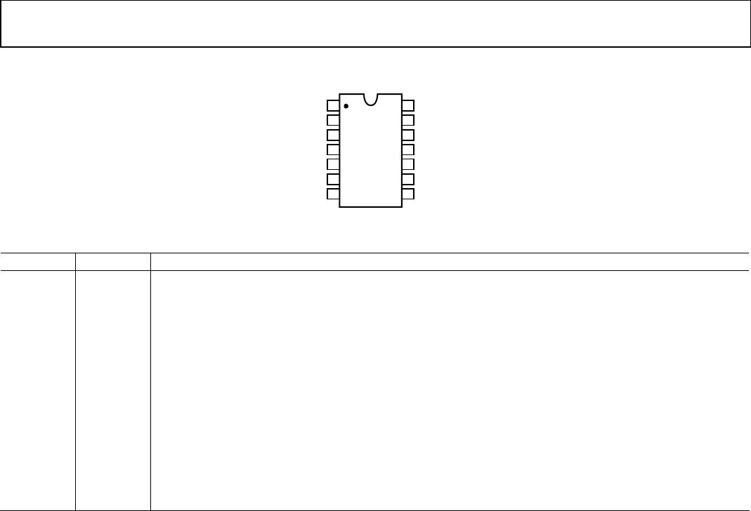
PIN CONFIGURATION AND FUNCTION DESCRIPTIONS
AD734
TOP VIEW
(Not to Scale)
X1
1
X2
2
U0
3
U1
4
U2
5
VP
DD
W
Z1
Z2
14
13
12
11
10
Y1
6
Y2
7
ER
VN
9
8
00827-001
Figure 3. 14-Lead PDIP and 14-Lead CERDIP
Table 4. Pin Function Descriptions
Pin No. Mnemonic Description
1 X1 X Differential Multiplicand Input.
2 X2 X Differential Multiplicand Input.
3 U0 Denominator Current Source Enable Interface.
4 U1 Denominator Interface—see the Functional Description section.
5 U2 Denominator Interface—see the Functional Description section.
6 Y1 Y Differential Multiplicand Input.
7 Y2 Y Differential Multiplicand Input.
8 VN Negative Supply.
9 ER Reference Voltage.
10 Z2 Z Differential Summing Input.
11 Z1 Z Differential Summing Input.
12 W Output.
13 DD Denominator Disable.
14 VP Positive Supply.