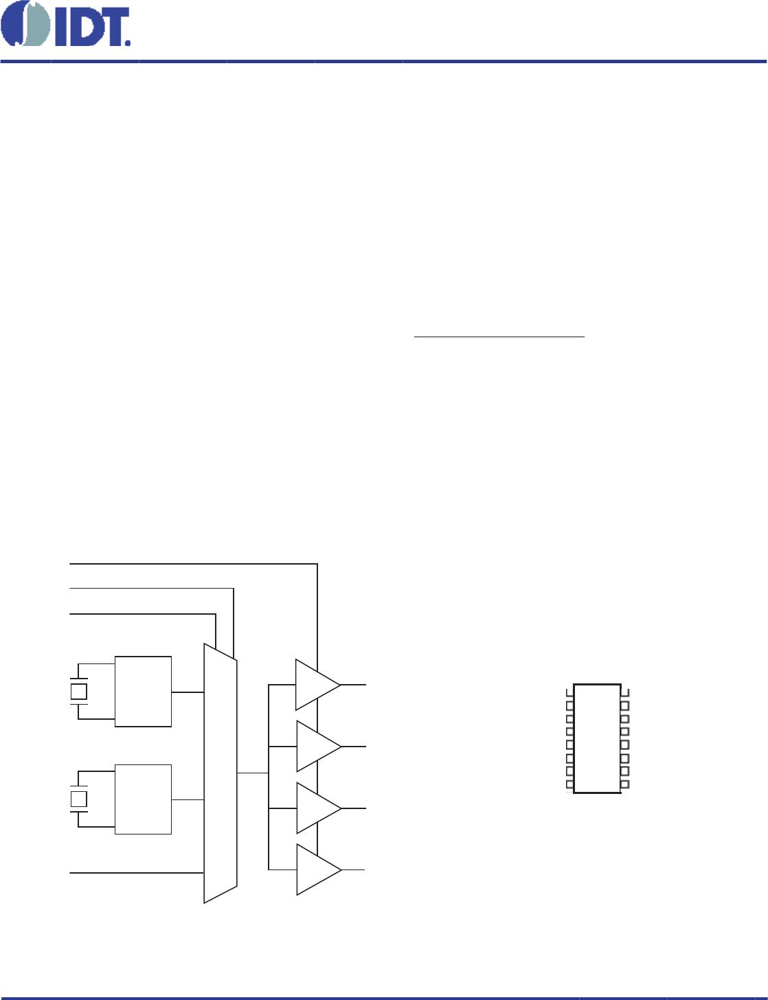
Low Skew, 1-to-4, Crystal-to-LVCMOS/
LVTTL Fanout Buffer
83904-02
Data Sheet
©2016 Integrated Device Technology, Inc Revision A March 17, 20161
FEATURES
Four LVCMOS/LVTTL outputs,
19Ω typical output impedance
@ V
DD
= V
DDO
= 3.3V
Two Crystal oscillator input pairs
One LVCMOS/LVTTL clock input
Crystal input frequencry range: 12MHz – 38.88MHz
Output frequency: 200MHz (maximum)
Output Skew: 40ps (maximum) @ V
DD
= V
DDO
= 3.3V
RMS phase jitter @ 25MHz output, using a 25MHz crystal
(100Hz – 1MHz): 0.16ps (typical) @ V
DD
= V
DDO
= 3.3V
RMS phase noise at 25MHz:
Offset Noise Power
100Hz ..............-118.4 dBc/Hz
1kHz ..............-141.5 dBc/Hz
10kHz ..............-157.2 dBc/Hz
100kHz ..............-157.2 dBc/Hz
Supply Voltage Modes:
(Core/Output)
3.3V/3.3V
3.3V/2.5V
3.3V/1.8V
2.5V/2.5V
2.5V/1.8V
0°C to 70°C ambient operating temperature
Available in lead-free (RoHS 6) package
GENERAL DESCRIPTION
The 83904-02 is a low skew, high performance 1-to-4 Crystal-to-
LVCMOS Fanout Buffer. The 83904-02 has selectable single-ended
clock or two crystal-oscillator inputs. There is an output enable to
disable the outputs by placing them into a high-impedance state.
Guaranteed output and part-to-part skew characteristics
make the 83904-02 ideal for those applications demand-
ing well defi ned performance and repeatability.
BLOCK DIAGRAM
OE
CLK_SEL0
CLK_SEL1
CLK
Q0
Q1
Q2
Q3
OSC
OSC
0 0
0 1
1 0
1 1
Pullup
83904-02
16-Lead TSSOP
4.4mm x 5.0mm x 0.92mm
package body
G Package
Top View
Pulldown
Pulldown
XTAL_IN0
XTAL_OUT0
XTAL_IN1
XTAL_OUT1
Pulldown
CLK_SEL0
XTAL_OUT0
XTAL_IN0
V
DD
XTAL_IN1
XTAL_OUT1
CLK_SEL1
CLK
1
2
3
4
5
6
7
8
16
15
14
13
12
11
10
9
V
DDO
Q0
Q1
GND
Q2
Q3
V
DDO
OE
PIN ASSIGNMENT
83904-02 Data Sheet
©2016 Integrated Device Technology, Inc Revision A March 17, 20162
TABLE 1. PIN DESCRIPTIONS
TABLE 2. PIN CHARACTERISTICS
Number Name Type Description
1, 7
CLK_SEL0,
CLK_SEL1
Input Pulldown
Clock select inputs. See Table 3, Input Reference Function Table.
LVCMOS / LVTTL interface levels.
2, 3
XTAL_OUT0,
XTAL_IN0
Input
Crystal oscillator interface. XTAL_IN0 is the input.
XTAL_OUT0 is the output.
4V
DD
Power Positive supply pin.
5, 6
XTAL_IN1,
XTAL_OUT1
Input
Crystal oscillator interface. XTAL_IN1 is the input.
XTAL_OUT1 is the output.
8 CLK Input Pulldown Single-ended clock input. LVCMOS/LVTTL interface levels.
9 OE Input Pullup
Output enable. When LOW, outputs are in HIGH impedance state.
When HIGH, outputs are active. LVCMOS / LVTTL interface levels.
10, 16 V
DDO
Power Output supply pins.
11, 12, 14, 15 Q3, Q2, Q1, Q0 Output Single-ended clock outputs. LVCMOS/LVTTL interface levels.
13 GND Power Power supply ground.
NOTE: Pullup and Pulldown refer to internal input resistors. See Table 2, Pin Characteristics, for typical values.
TABLE 3. INPUT REFERENCE FUNCTION TABLE
Symbol Parameter Test Conditions Minimum Typical Maximum Units
C
IN
Input Capacitance 4 pF
R
PULLUP
Input Pullup Resistor 51
kΩ
R
PULLDOWN
Input Pulldown Resistor 51
kΩ
C
PD
Power Dissipation Capacitance
(per output)
V
DDO
= 3.465V 8 pF
V
DDO
= 2.625V 7 pF
V
DDO
= 2.0V 7 pF
R
OUT
Output Impedance
V
DDO
= 3.3V 19
Ω
V
DDO
= 2.5V 21
Ω
V
DDO
= 1.8V 32
Ω
Control Inputs
Reference
CLK_SEL1 CLK_SEL0
0 0 XTAL0 (default)
0 1 XTAL1
1 0 CLK
1 1 CLK
83904-02 Data Sheet
©2016 Integrated Device Technology, Inc Revision A March 17, 20163
ABSOLUTE MAXIMUM RATINGS
Supply Voltage, V
DD
4.6V
Inputs, V
I
-0.5V to V
DD
+ 0.5 V
Outputs, V
O
-0.5V to V
DDO
+ 0.5V
Package Thermal Impedance, θ
JA
100.3°C/W (0 mps)
Storage Temperature, T
STG
-65°C to 150°C
NOTE: Stresses beyond those listed under Absolute
Maximum Ratings may cause permanent damage to the
device. These ratings are stress specifi cations only. Functional
operation of product at these conditions or any conditions beyond
those listed in the DC Characteristics or AC Characteristics is not
implied. Exposure to absolute maximum rating conditions for ex-
tended periods may affect product reliability.
TABLE 4A. POWER SUPPLY DC CHARACTERISTICS, V
DD
= V
DDO
= 3.3V±5%, TA = 0°C TO 70°C
TABLE 4D. POWER SUPPLY DC CHARACTERISTICS, V
DD
= V
DDO
= 2.5V±5%, TA = 0°C TO 70°C
TABLE 4B. POWER SUPPLY DC CHARACTERISTICS, V
DD
= 3.3V±5%, V
DDO
= 2.5V±5%, TA = 0°C TO 70°C
TABLE 4C. POWER SUPPLY DC CHARACTERISTICS, V
DD
= 3.3V±5%, V
DDO
= 1.8V±0.2V, TA = 0°C TO 70°C
Symbol Parameter Test Conditions Minimum Typical Maximum Units
V
DD
Power Supply Voltage 3.135 3.3 3.465 V
V
DDO
Output Supply Voltage 3.135 3.3 3.465 V
I
DD
Power Supply Current
No Load & XTALx selected @ 12MHz 7 mA
No Load & CLK selected 1 mA
I
DDO
Output Supply Current No Load & CLK selected 1 mA
Symbol Parameter Test Conditions Minimum Typical Maximum Units
V
DD
Power Supply Voltage 3.135 3.3 3.465 V
V
DDO
Output Supply Voltage 2.375 2.5 2.625 V
I
DD
Power Supply Current
No Load & XTALx selected @ 12MHz 7 mA
No Load & CLK selected 1 mA
I
DDO
Output Supply Current No Load & CLK selected 1 mA
Symbol Parameter Test Conditions Minimum Typical Maximum Units
V
DD
Power Supply Voltage 3.135 3.3 3.465 V
V
DDO
Output Supply Voltage 1.6 1.8 2.0 V
I
DD
Power Supply Current
No Load & XTALx selected @ 12MHz 7 mA
No Load & CLK selected 1 mA
I
DDO
Output Supply Current No Load & CLK selected 1 mA
Symbol Parameter Test Conditions Minimum Typical Maximum Units
V
DD
Power Supply Voltage 2.375 2.5 2.625 V
V
DDO
Output Supply Voltage 2.375 2.5 2.625 V
I
DD
Power Supply Current
No Load & XTALx selected @ 12MHz 3 mA
No Load & CLK selected 1 mA
I
DDO
Output Supply Current No Load & CLK selected 1 mA

83904AG-02LF

Mfr. #:
Manufacturer:
IDT
Description:
Clock Buffer Fanout Buffer,2-XTAL /LVCMOS Input
Lifecycle:
New from this manufacturer.
Delivery:
DHL FedEx Ups TNT EMS
Payment:
T/T Paypal Visa MoneyGram Western Union

Products related to this Datasheet