83904-02 Data Sheet
©2016 Integrated Device Technology, Inc Revision A March 17, 20167
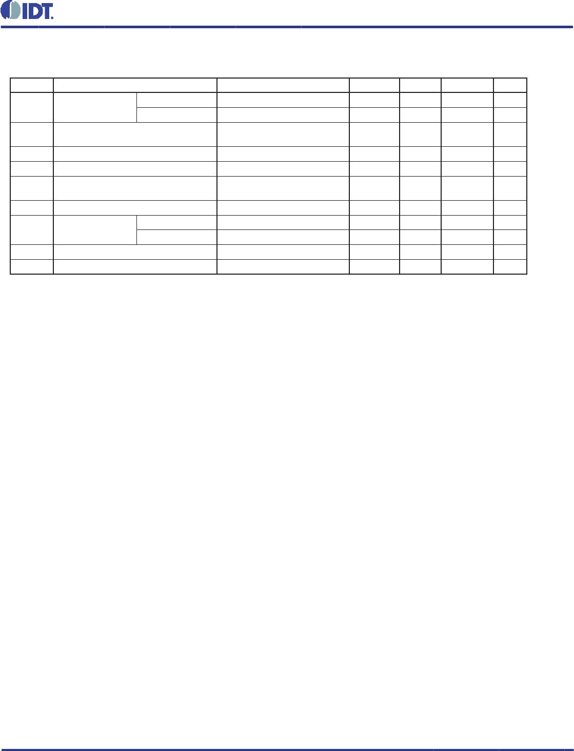
TABLE 6E. AC CHARACTERISTICS, V
DD
= 2.5V ± 5%, V
DDO
= 1.8V±0.2V, TA = 0°C TO 70°C
Symbol Parameter Test Conditions Minimum Typical Maximum Units
f
MAX
Output Frequency
w/external XTAL 12 38.88 MHz
w/external CLK 200 MHz
tp
LH
Propagation Delay, Low-to-High; NOTE
1
1.7 2.5 3.3 ns
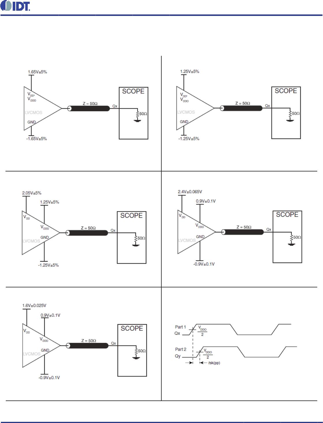
tsk(o) Output Skew; NOTE 2 40 ps
tsk(pp) Part-to-Part Skew; NOTE 2, 3 700 ps
tjit(Ø)
RMS Phase Jitter, Random;
NOTE 2, 4
25MHz, Integration Range:
100Hz - 1MHz
0.19 ps
t
R
/ t
F
Output Rise/Fall Time 20% to 80% 100 1000 ps
odc
Output
Duty Cycle
w/external XTAL 45 55 %
w/external CLK ƒ < 150MHz 46 54 %
t
EN
Output Enable Time; NOTE 5 10 ns
t
DIS
Output Disable Time; NOTE 5 10 ns
NOTE 1: Measured from V
DD
/2 of the input to V
DDO
/2 of the output.
NOTE 2: This parameter is defi ned in accordance with JEDEC Standard 65.
NOTE 3: Defi ned as skew between outputs on different devices operating a the same supply voltages and
with equal load conditions. Using the same type of input on each device, the output is measured at V
DDO
/2.
NOTE 4: Phase jitter is dependent on the input source used.
NOTE 5: These parameters are guaranteed by characterization. Not tested in production.