Features
• Low-voltage Operation
–1.8V (V
CC
= 1.8V to 3.6V)
–2.5V (V
CC
= 2.5V to 5.5V)
• Internally Organized 131,072 x 8
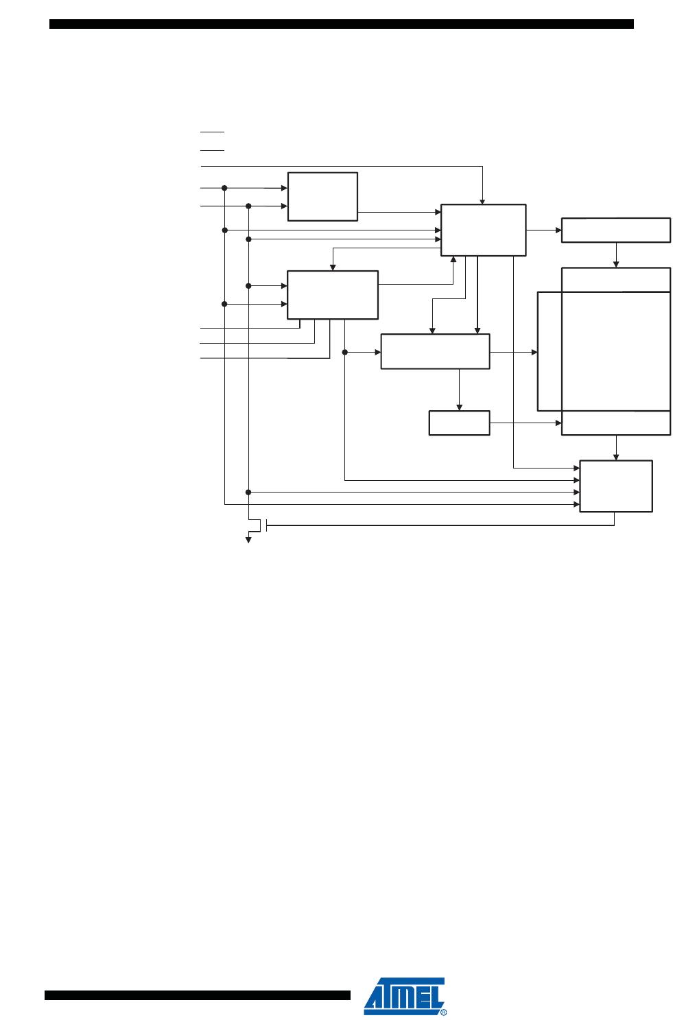
• Two-wire Serial Interface
• Schmitt Triggers, Filtered Inputs for Noise Suppression
• Bidirectional Data Transfer Protocol
• 400 kHz (1.8V) and 1 MHz (5V, 2.5V) Clock Rate
• Write Protect Pin for Hardware and Software Data Protection
• 256-byte Page Write Mode (Partial Page Writes Allowed)
• Random and Sequential Read Modes
• Self-timed Write Cycle (5 ms Typical)
• High Reliability
– Endurance: 1,000,000 Write Cycles/Page
– Data Retention: 40 Years
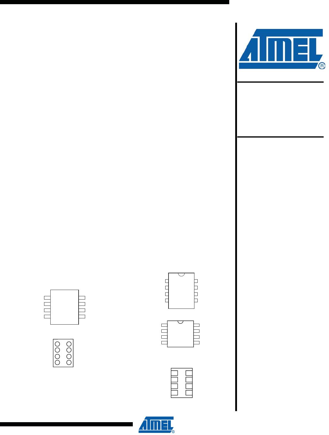
• 8-lead PDIP, 8-lead JEDEC SOIC, 8-lead EIAJ SOIC, 8-lead TSSOP, 8-lead Ultra Thin
Small Array (SAP), and 8-ball dBGA2 Packages
• Die Sales: Wafer Form, Tape and Reel and Bumped Die
Description
The AT24C1024B provides 1,048,576 bits of serial electrically erasable and program-
mable read only memory (EEPROM) organized as 131,072 words of 8 bits each. The
device’s cascadable feature allows up to four devices to share a common two-wire
bus. The device is optimized for use in many industrial and commercial applications
where low-power and low-voltage operation are essential. The devices are available
in space-saving 8-lead PDIP, 8-lead JEDEC SOIC, 8-lead EIAJ SOIC, 8-lead TSSOP,
8-ball dBGA2 and 8-lead Ultra Thin SAP packages. In addition, the entire family is
available in 1.8V (1.8V to 3.6V) and 2.5V (2.5V to 5.5V) versions.
Two-wire Serial
EEPROM
1M (131,072 x 8)
AT24C1024B
with Two Device
Address Inputs
Rev. 5194F–SEEPR–1/08
8-lead PDIP
1
2
3
4
8
7
6
5
NC
A1
A2
GND
VCC
WP
SCL
SDA
8-lead TSSOP
1
2
3
4
8
7
6
5
VCC
WP
SCL
SDA
NC
A1
A2
GND
8-lead SOIC
1
2
3
4
8
7
6
5
NC
A1
A2
GND
VCC
WP
SCL
SDA
8-lead Ultra-Thin SAP
Bottom View
VCC
WP
SCL
SDA
NC
A1
A2
GND
1
2
3
4
8
7
6
5
8-lead dBGA2
Bottom View
VCC
WP
SCL
SDA
NC
A1
A2
GND
1
2
3
4
8
7
6
5