9
5194F–SEEPR–1/08
AT24C1024B
DATA SECURITY: The AT24C1024B has a hardware data protection scheme that allows the
user to write-protect the entire memory when the WP pin is at V
CC
.
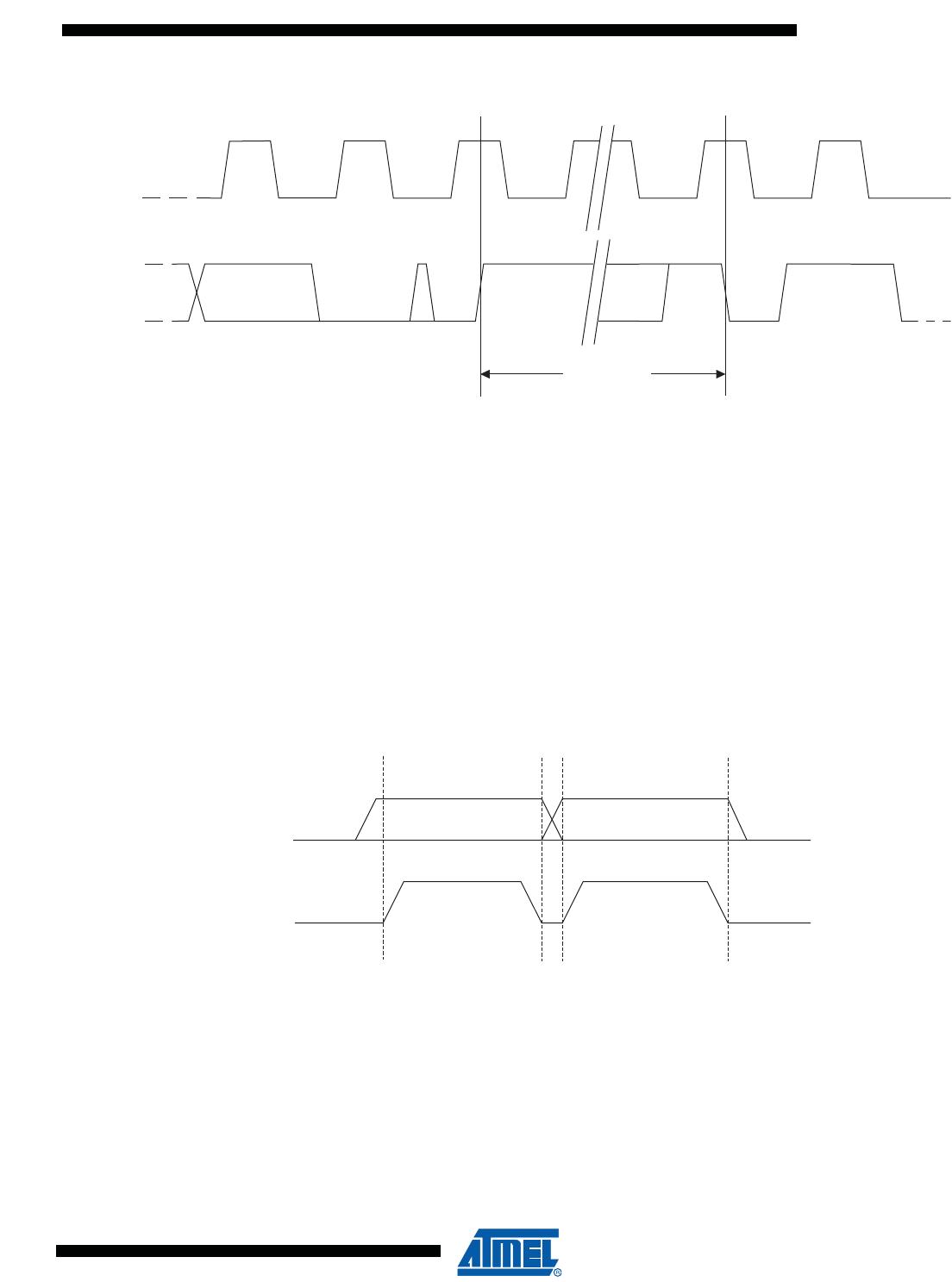
6. Write Operations
BYTE WRITE: To select a data word in the 1024K memory requires a 17-bit word address. The
word address field consists of the P
0
bit of the device address, then the most significant word
address followed by the least significant word address (see Figure 7-2 on page 11)
A write operation requires the P
0
bit and two 8-bit data word addresses following the device
address word and acknowledgment. Upon receipt of this address, the EEPROM will again
respond with a zero and then clock in the first 8-bit data word. Following receipt of the 8-bit data
word, the EEPROM will output a zero. The addressing device, such as a microcontroller, then
must terminate the write sequence with a stop condition. At this time the EEPROM enters an
internally timed write cycle, T
WR
, to the nonvolatile memory. All inputs are disabled during this
write cycle and the EEPROM will not respond until the write is complete (see Figure 7-2 on page
11).
PAGE WRITE: The 1024K EEPROM is capable of 256-byte page writes.
A page write is initiated the same way as a byte write, but the microcontroller does not send a
stop condition after the first data word is clocked in. Instead, after the EEPROM acknowledges
receipt of the first data word, the microcontroller can transmit up to 255 more data words. The
EEPROM will respond with a zero after each data word received. The microcontroller must ter-
minate the page write sequence with a stop condition (see Figure 7-3 on page 11).
The data word address lower 8 bits are internally incremented following the receipt of each data
word. The higher data word address bits are not incremented, retaining the memory page row
location. When the word address, internally generated, reaches the page boundary, the follow-
ing byte is placed at the beginning of the same page. If more than 256 data words are
transmitted to the EEPROM, the data word address will “roll over” and previous data will be
overwritten. The address “rollover” during write is from the last byte of the current page to the
first byte of the same page.
ACKNOWLEDGE POLLING: Once the internally timed write cycle has started and the
EEPROM inputs are disabled, acknowledge polling can be initiated. This involves sending a
start condition followed by the device address word. The read/write bit is representative of the
operation desired. Only if the internal write cycle has completed will the EEPROM respond with
a zero, allowing the read or write sequence to continue.
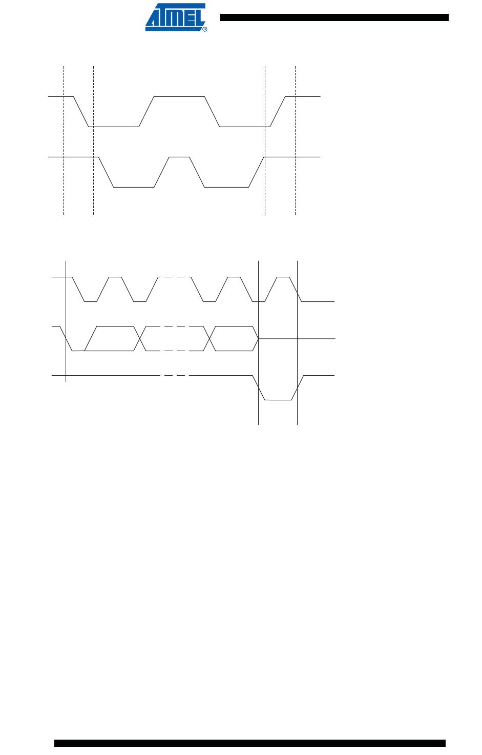
7. Read Operations
Read operations are initiated the same way as write operations with the exception that the
read/write select bit in the device address word is set to one. There are three read operations:
current address read, random address read and sequential read.
CURRENT ADDRESS READ: The internal data word address counter maintains the last
address accessed during the last read or write operation, incremented by one. This address
stays valid between operations as long as the chip power is maintained. The address “rollover”
during read is from the last byte of the last memory page, to the first byte of the first page.