4
5194F–SEEPR–1/08
AT24C1024B
3. Memory Organization
AT24C1024B, 1024K SERIAL EEPROM: The 1024K is internally organized as 512 pages of
256 bytes each. Random word addressing requires a 17-bit data word address.
Note: 1. This parameter is characterized and is not 100% tested.
Note: 1. V
IL
min and V
IH
max are reference only and are not tested.
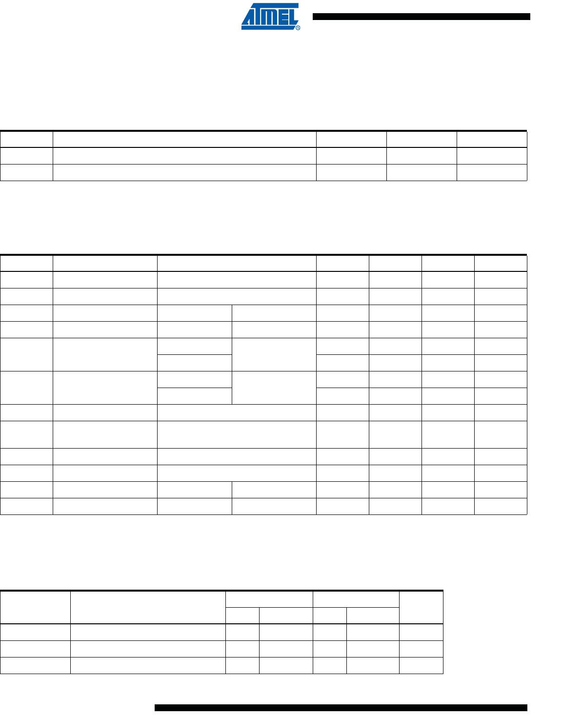
Table 3-1. Pin Capacitance
(1)
Applicable over recommended operating range from T
A
= 25qC, f = 1.0 MHz, V
CC
= +1.8V
Symbol Test Condition Max Units Conditions
C
I/O
Input/Output Capacitance (SDA) 8 pF V
I/O
= 0V
C
IN
Input Capacitance (A
1
, SCL) 6 pF V
IN
= 0V
Table 3-2. DC Characteristics
Applicable over recommended operating range from: T
AI
= –40qC to +85qC, V
CC
= +1.8V to +5.5V (unless otherwise noted)
Symbol Parameter Test Condition Min Typ Max Units
V
CC1
Supply Voltage 1.8 3.6 V
V
CC2
Supply Voltage 2.5 5.5 V
I
CC
Supply Current V
CC
= 5.0V READ at 400 kHz 2.0 mA
I
CC
Supply Current V
CC
= 5.0V WRITE at 400 kHz 3.0 mA
I
SB1
Standby Current
V
CC
= 1.8V
V
IN
= V
CC
or V
SS
1.0 A
V
CC
= 3.6V 3.0 A
I
SB2
Standby Current
V
CC
= 2.5V
V
IN
= V
CC
or V
SS
2.0 A
V
CC
= 5.5V 6.0 A
I
LI
Input Leakage Current V
IN
= V
CC
or
V
SS
0.10 3.0 A
I
LO
Output Leakage
Current
V
OUT
= V
CC
or
V
SS
0.05 3.0 A
V
IL
Input Low Level
(1)
–0.6 V
CC
x 0.3 V
V
IH
Input High Level
(1)
V
CC
x 0.7 V
CC
+ 0.5 V
V
OL1
Output Low Level V
CC
= 1.8V I
OL
= 0.15 mA 0.2 V
V
OL2
Output Low Level V
CC
= 3.0V I
OL
= 2.1 mA 0.4 V
Table 3-3. AC Characteristics (Industrial Temperature)
Applicable over recommended operating range from T
AI
= 40qC to +85qC, V
CC
= +1.8V to +3.6V, CL = 100 pF (unless oth-
erwise noted). Test conditions are listed in Note 2.
Symbol Parameter
1.8-volt 2.5, 5.0-volt
UnitsMin Max Min Max
f
SCL
Clock Frequency, SCL 400 1000 kHz
t
LOW
Clock Pulse Width Low 1.3 0.4 s
t
HIGH
Clock Pulse Width High 0.6 0.4 s
5
5194F–SEEPR–1/08
AT24C1024B
Notes: 1. This parameter is ensured by characterization only.
2. AC measurement conditions:
R
L
(connects to V
CC
): 1.3 k: (2.5V, 5V), 10 k: (1.8V)
Input pulse voltages: 0.3 V
CC
to 0.7 V
CC
Input rise and fall times: d 50 ns
Input and output timing reference voltages: 0.5 V
CC
4. Device Operation
CLOCK and DATA TRANSITIONS: The SDA pin is normally pulled high with an external
device. Data on the SDA pin may change only during SCL low time periods (see Figure 4-4 on
page 7). Data changes during SCL high periods will indicate a start or stop condition as defined
below.
t
i
Noise Suppression Time
(1)
100 50 ns
t
AA
Clock Low to Data Out Valid 0.05 0.9 0.05 0.55 s
t
BUF
Time the bus must be free before a
new transmission can start
(1)
1.3 0.5 s
t
HD.STA
Start Hold Time 0.6 0.25 s
t
SU.STA
Start Set-up Time 0.6 0.25 s
t
HD.DAT
Data In Hold Time 0 0 s
t
SU.DAT
Data In Set-up Time 100 100 ns
t
R
Inputs Rise Time
(1)
0.3 0.3 s
t
F
Inputs Fall Time
(1)
300 100 ns
t
SU.STO
Stop Set-up Time 0.6 0.25 s
t
DH
Data Out Hold Time 50 50 ns
t
WR
Write Cycle Time 5 5 ms
Endurance
(1)
25°C, Page Mode, 3.3V 1,000,000
Write
Cycles
Table 3-3. AC Characteristics (Industrial Temperature)
Applicable over recommended operating range from T
AI
= 40qC to +85qC, V
CC
= +1.8V to +3.6V, CL = 100 pF (unless oth-
erwise noted). Test conditions are listed in Note 2.
Symbol Parameter
1.8-volt 2.5, 5.0-volt
UnitsMin Max Min Max
6
5194F–SEEPR–1/08
AT24C1024B
START CONDITION: A high-to-low transition of SDA with SCL high is a start condition which
must precede any other command (see Figure 4-5 on page 8).
STOP CONDITION: A low-to-high transition of SDA with SCL high is a stop condition. After a
read sequence, the Stop command will place the EEPROM in a standby power mode (see Fig-
ure 4-5 on page 8).
ACKNOWLEDGE: All addresses and data words are serially transmitted to and from the
EEPROM in 8-bit words. The EEPROM sends a zero during the ninth clock cycle to acknowl-
edge that it has received each word.
STANDBY MODE: The AT24C1024B features a low-power standby mode which is enabled: a)
upon power-up and b) after the receipt of the stop bit and the completion of any internal
operations.
SOFTWARE RESET: After an interruption in protocol, power loss or system reset, any 2-wire
part can be protocol reset by following these steps: (a) Create a start bit condition, (b) clock 9
cycles, (c) create another start bit followed by stop bit condition as shown below. The device is
ready for next communication after above steps have been completed.
Figure 4-1. Software Reset
Figure 4-2. Bus Timing (SCL: Serial Clock, SDA: Serial Data I/O
®
)
Start bit
Stop bitStart bitDummy Clock Cycles
SCL
SDA
123 89
SCL
SDA IN
SDA OUT
t
F
t
HIGH
t
LOW
t
LOW
t
R
t
AA
t
DH
t
BUF
t
SU.STO
t
SU.DAT
t
HD.DAT
t
HD.STA
t
SU.STA

AT24C1024B-TH-B

Mfr. #:
Manufacturer:
Microchip Technology / Atmel
Description:
EEPROM 1.8V - NiPdAu 1.8V
Lifecycle:
New from this manufacturer.
Delivery:
DHL FedEx Ups TNT EMS
Payment:
T/T Paypal Visa MoneyGram Western Union