General Description
The MAX8563/MAX8564/MAX8564A ultra-low-output dual
and triple LDO controllers allow flexible and inexpensive
point-of-load voltage conversion in motherboards,
desknotes, notebooks, and other applications.
These parts feature a 0.5V reference voltage with ±1%
accuracy providing tight regulation of the output volt-
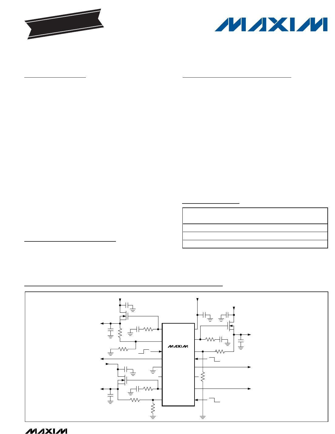
age. The MAX8563 has three n-channel MOSFET con-
troller outputs, and the MAX8564/MAX8564A has two
controller outputs.
Each controller output is adjustable from 0.5V to 3.3V
when V
DD
= 12V and between 0.5V and 1.8V when V
DD
= 5V. Each output is independently enabled and asserts
a POK signal when the output reaches 94% of the set
value. Each output is protected against a soft short-circuit
condition by an undervoltage comparator that disables
the output when it drops to under 80% of the set voltage
for more than 50µs. For a catastrophic short condition, the
regulators are shut down immediately if the output drops
below 60% of the set voltage.
The MAX8563 is available in a 16-pin QSOP
package, and the MAX8564/MAX8564A are available
in a 10-pin µMAX
®
package.
Applications
Features
MAX8563: 3 Outputs
MAX8564/MAX8564A: 2 Outputs
±1% Feedback Regulation
Adjustable Output Voltage Down to 0.5V
Can Use Ceramic Output Capacitors
Wide Supply Voltage Range Permits Operation
from 5V or 12V Rails
Individual Enable Control and POK Signal Allows
Sequencing
Overload Protection Against Soft Short-Circuit
Condition
Undervoltage Short-Circuit Protection
Drive n-Channel MOSFETs
MAX8563/MAX8564/MAX8564A
±1%, Ultra-Low Output Voltage, Dual and Triple
Linear n-FET Controllers
________________________________________________________________ Maxim Integrated Products 1
Ordering Information
19-3290; Rev 2; 6/06
For pricing, delivery, and ordering information, please contact Maxim/Dallas Direct! at
1-888-629-4642, or visit Maxim’s website at www.maxim-ic.com.
EVALUATION KIT
AVAILABLE
PART
TEMP RANGE
PIN-
PACKAGE
PKG
CODE
MAX8563EEE
-40°C to +85°C
16 QSOP E16-1
MAX8564EUB
-40°C to +85°C
10 µMAX U10-2
MAX8564AEUB+ -40°C to +85°C
10 µMAX U10-2
OFF
ON
OFF
ON
OFF
ON
DRV1
FB1
EN1
POK1
GND
N.C.
DRV3
FB3
V
DD
DRV2
FB2
EN2
POK2
N.C.
POK3
EN3
MAX8563
1.8V ±5% IN
C1
C5
R2
R1
C4
OUT1
1.5V/1.5A
R3
Q1
POK1
3.3V ±5% IN
OUT3
2.5V/2A*
C9
C10
C8
Q3
R8
R7
R9
R6
R5
R4
C6
C2 C3
C7
Q2
OUT2
1.05V/3A
POK2
POK3
5V OR 12V
IN
1.2V ±5% IN
*2.5V OUTPUT ONLY WITH V
DD
= 12V
Typical Operating Circuit
Pin Configurations appear at end of data sheet.
µMAX is a registered trademark of Maxim Integrated Products, Inc.
+Denotes lead-free package.
Motherboards
Dual/Triple Power Supplies
Desknotes and Notebooks
Graphic Cards
Ultra-Low-Dropout
Voltage Regulators
Low-Voltage DSP, µP, and
Microcontroller Power
Supplies
MAX8563/MAX8564/MAX8564A
±1%, Ultra-Low Output Voltage, Dual and Triple
Linear n-FET Controllers
2 _______________________________________________________________________________________
ABSOLUTE MAXIMUM RATINGS
ELECTRICAL CHARACTERISTICS
(V
DD
= V
EN1
= V
EN2
= V
EN3
= 5V, V
GND
= 0V, T
A
= -40°C to +85°C, unless otherwise noted. Typical values are at T
A
= +25°C.) (Note 1)
Stresses beyond those listed under “Absolute Maximum Ratings” may cause permanent damage to the device. These are stress ratings only, and functional
operation of the device at these or any other conditions beyond those indicated in the operational sections of the specifications is not implied. Exposure to
absolute maximum rating conditions for extended periods may affect device reliability.
V
DD
to GND............................................................-0.3V to +14V
DRV1, DRV2, DRV3, EN1, EN2,
EN3 to GND............................................-0.3V to (V
DD
+ 0.3V)
FB1, FB2, FB3, POK1, POK2, POK3 to GND ...........-0.3V to +6V
Continuous Power Dissipation (T
A
= +70°C)
10-Pin µMAX (derate 5.6mW/°C above +70°C) ........444.4mW
16-Pin QSOP (derate 8.3mW/°C above +70°C)........666.7mW
Operating Temperature Range ...........................-40°C to +85°C
Junction Temperature......................................................+150°C
Storage Temperature Range .............................-65°C to +150°C
Lead Temperature (soldering, 10s) .................................+300°C
PARAMETER CONDITIONS
MIN TYP MAX
UNITS
GENERAL
V
DD
Voltage Range 4.5
13.2
V
V
DD
Undervoltage-Lockout Threshold Rising, 200mV hysteresis (typ)
3.56 3.76 4.00
V
V
EN_
= V
DD
= 12V (MAX8563)
930 1600
V
DD
Quiescent Current
V
EN_
= V
DD
= 12V (MAX8564/MAX8564A)
660 1200
µA
V
DD
Shutdown Current EN1 = EN2 = EN3 = GND, V
DD
= 12V 25 µA
LDOs
T
A
= 0°C to +85°C
0.494
0.5
0.504
FB_ Accuracy
T
A
= -40°C to +85°C
0.489 0.509
V
T
A
= +25°C
-100 +100
FB_ Input Bias Current
T
A
= +85°C -8
nA
MAX8563, MAX8564
100
DRV_ Soft-Start Charging Current
MAX8564A 10
µA
T
A
= 0°C to +85°C 4
DRV_ Max Sourcing Current V
FB_
= 0.45V
T
A
= -40°C to +85°C 3 7
mA
T
A
= 0°C to +85°C 3
DRV_ Max Sinking Current V
FB_
= 0.6V
T
A
= -40°C to +85°C 1.8 7
mA
V
DD
= 5V, V
FB_
= 0.46V 4.7
DRV_ Max Voltage
V
DD
= 13.2V, V
FB_
= 0.46V 8.0
10.9
V
FB_ Slow Short-Circuit Threshold Measured at FB_ (falling)
400
mV
FB_ Fast Short-Circuit Threshold Measured at FB_ (falling)
300
mV
Slow Short-Circuit Timer 50 µs
FB_ to DRV_ Transconductance
0.115 0.24 0.460
Mho
LOGIC
EN_ Input Low Level 0.7 V
EN_ Input High Level 1.3 V
T
A
= +25°C -0.1 +0.1
EN_ Input Leakage Current
V
EN_
= 0 and V
DD
,
V
DD
= 13.2V
T
A
= +85°C 0.001
µA
MAX8563/MAX8564/MAX8564A
±1%, Ultra-Low Output Voltage, Dual and Triple
Linear n-FET Controllers
_______________________________________________________________________________________ 3
ELECTRICAL CHARACTERISTICS (continued)
(V
DD
= V
EN1
= V
EN2
= V
EN3
= 5V, V
GND
= 0V, T
A
= -40°C to +85°C, unless otherwise noted. Typical values are at T
A
= +25°C.) (Note 1)
PARAMETER CONDITIONS
MIN
MAX
UNITS
POK_ Threshold Falling Measured at FB_ (falling)
425 440
455 mV
POK_ Threshold Rising at Startup Measured at FB_ (rising)
455 470
485 mV
POK_ Output Low Level Sinking 1mA, V
DD
= 4.5V, V
FB_
= 0.4V 0.1 V
T
A
= +25°C
0.1
POK_ Output High Leakage V
DD
= 5.5V
T
A
= +85°C 0.001
µA
Note 1: Specifications are production tested at T
A
= +25°C. Maximum and minimum specifications over temperature are guaranteed by
design.
Typical Operating Characteristics
(Circuit of Figure 1, T
A
= +25°C.)
OUTPUT VOLTAGE vs. INPUT VOLTAGE
MAX8563 toc01
INPUT VOLTAGE (V)
OUTPUT VOLTAGE (V)
1.91.81.71.61.51.41.31.21.1
1.1
1.2
1.3
1.4
1.5
1.6
1.0
1.0 2.0
V
DD
= 5V
V
OUT1
V
OUT2
OUTPUT VOLTAGE vs. INPUT VOLTAGE
MAX8563 toc02
INPUT VOLTAGE (V)
OUTPUT VOLTAGE (V)
3.41.4 2.2 2.61.8 3.0
1.2
1.4
1.6
1.8
2.0
2.2
2.4
2.6
1.0
1.0
V
DD
= 12V
V
OUT3
V
OUT1
V
OUT2
OUTPUT VOLTAGE vs. OUTPUT CURRENT
MAX8563 toc03
OUTPUT CURRENT (A)
OUTPUT VOLTAGE (V)
2.52.01.51.00.5
1.1
1.2
1.3
1.4
1.5
1.6
1.7
1.8
1.9
2.0
2.1
2.2
2.3
2.4
2.5
2.6
1.0
03.0
V
DD
= 12V
V
OUT3
V
OUT1
V
OUT2
FEEDBACK VOLTAGE
vs. TEMPERATURE
MAX8563 toc04
TEMPERATURE (°C)
FEEDBACK VOLTAGE (V)
603510-15
0.4988
0.4990
0.4992
0.4994
0.4996
0.4998
0.5000
0.4986
-40 85
V
DD
= 5V
V
DD
= 12V
PSRR vs. FREQUENCY
MAX8563 toc05
FREQUENCY (Hz)
PSRR (dB)
10k1k
10
30
40
20
50
60
70
80
90
100
0
100 100k
V
OUT1
= 1.5V
V
IN1
= 2V
LOAD = 1.25Ω
V
DD
= 12V
LOAD TRANSIENT
MAX8563 toc06
I
OUT2
V
DRV2
V
IN2
V
OUT2
20mV/div
AC-COUPLED
2V/div
200mV/div
AC-COUPLED
2A/div
0
10μs/div
0
V
DD
= 12V
FIGURE 1, C7 = 100μF 6TPE100MI

MAX8564AEUB+

Mfr. #:
Manufacturer:
Maxim Integrated
Description:
LDO Voltage Controllers Dual & Triple Linear n-FET Controller
Lifecycle:
New from this manufacturer.
Delivery:
DHL FedEx Ups TNT EMS
Payment:
T/T Paypal Visa MoneyGram Western Union