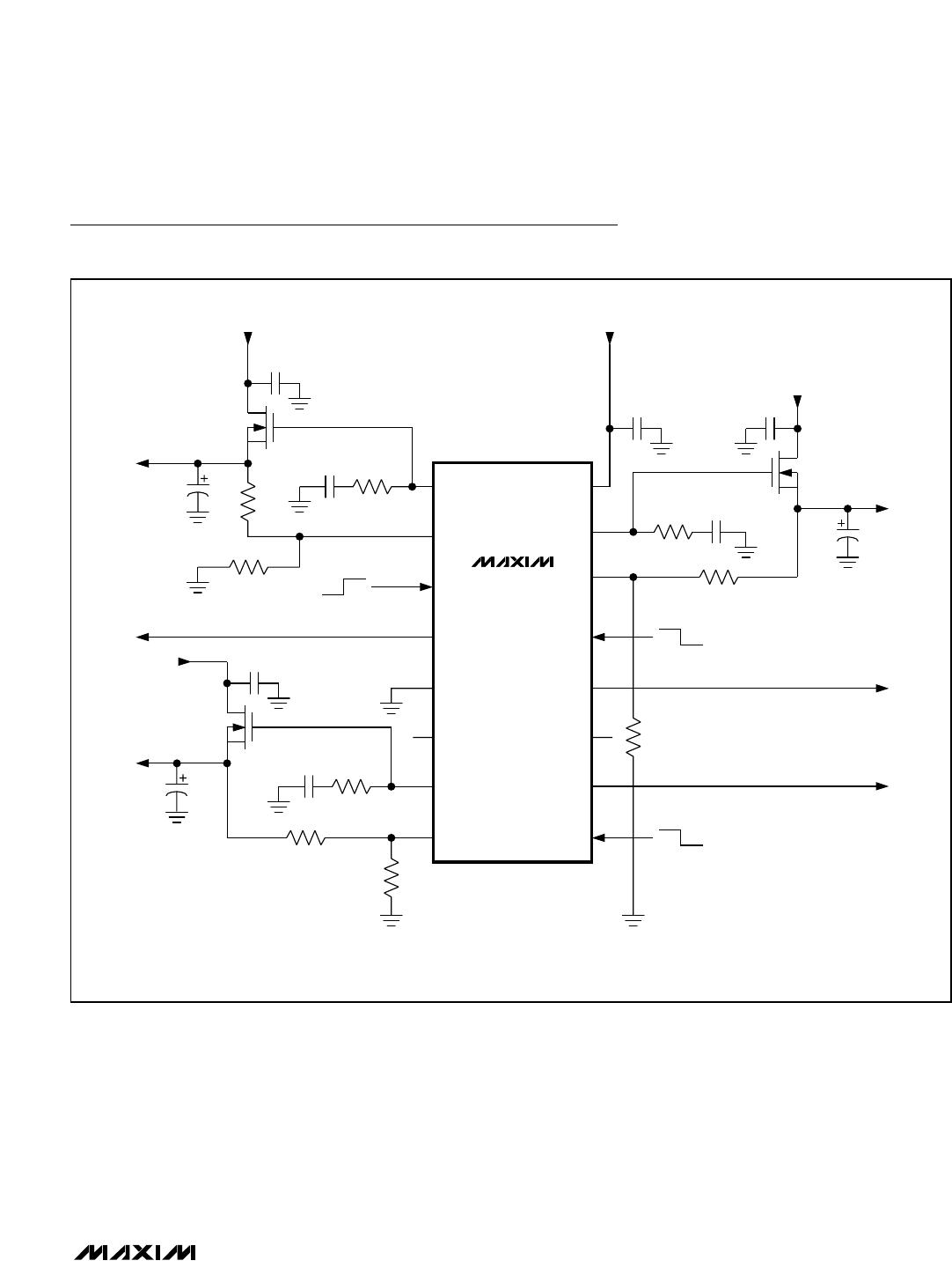
Detailed Description
The MAX8563/MAX8564/MAX8564A triple and dual
LDO controllers allow flexible and inexpensive voltage
conversion by controlling the gate of an external
n-MOSFET in a source-follower configuration. The
MAX8563/MAX8564/MAX8564A consist of multiple
identical LDO controllers. Each LDO controller features
an enable input (EN_) and a power-OK output (POK_).
The MAX8563/MAX8564/MAX8564A also include a 0.5V
reference, an internal regulator, and an undervoltage
lockout (UVLO). The transconductance amplifier mea-
sures the feedback voltage on FB_ and compares it to
an internal 0.5V reference connected to the positive
input. If the voltage on FB_ is lower than 0.5V, the cur-
rent output on the gate-drive output DRV_ is increased.
If the voltage on FB_ is higher than 0.5V, the current out-
put on the gate-drive output is decreased.
Bias Voltage (V
DD
), UVLO, and Soft-Start
The MAX8563/MAX8564/MAX8564A bias current
for internal circuitry is supplied by V
DD
. The V
DD
voltage
range is from 4.5V to 13.2V. If V
DD
drops below 3.76V
(typ), the MAX8563/MAX8564/MAX8564A assume that
the supply and reference voltages are too low and acti-
vate the UVLO circuitry. During UVLO, the internal regu-
lator (VL) and the internal bandgap reference are forced
off, DRV_ is pulled to GND, and POK_ is pulled low.
Before any internal startup circuitry is activated, V
DD
must
be above the UVLO threshold. After UVLO indicates that
V
DD
is high enough, the internal VL regulator, the internal
bandgap reference, and the bias currents are activated.
If EN_ is logic-high after the internal reference and bias
currents are activated, then the corresponding DRV_ out-
put initiates operation in soft-start mode. Once the voltage
on FB_ reaches 94% of the regulation threshold, the full
output current of the LDO controller is permitted.
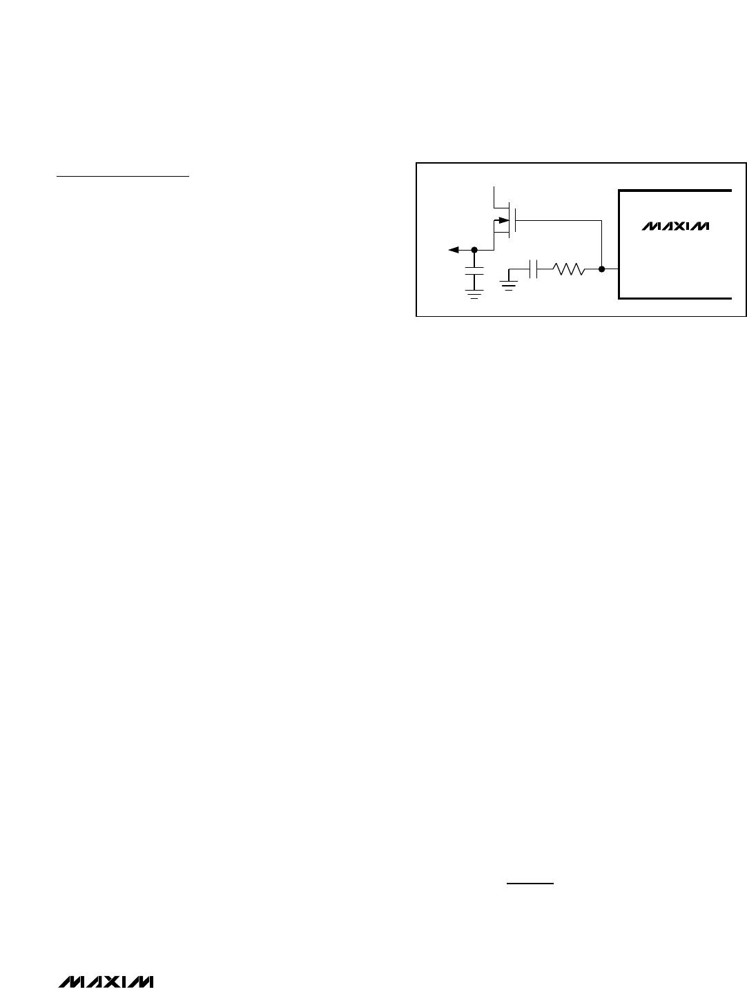
When an LDO is activated, the respective DRV_ is pulled
up from GND with a typical soft-start current of DRV soft-
start. The soft-start current limits the slew of the output
voltage and limits the initial spike of current that the drain
of the external n-MOSFET receives. The size of the com-
pensation capacitor (C
C
) limits the slew rate (see Figure
3). This output voltage slew rate is equal to (DRV_soft-
start /C
C
)mV/ms, where C
C
is in µF. The maximum startup
drain current is the ratio of C
OUT
to C
C
multiplied by the
soft-start current.
Input Voltage (Drain Voltage of the
External n-MOSFET)
The minimum input voltage to the drain of the n-MOSFET
is a function of the desired output voltage and the
dropout voltage of the n-MOSFET. Details on calculating
this value are covered in the Power MOSFET Selection
section.
The maximum input voltage to the drain of the n-MOSFET
is a function of the breakdown voltage and the thermal
conditions during operation. The breakdown voltage from
drain to source is normally provided in the MOSFET data
sheet. The theoretical maximum input voltage is the set
output voltage plus the breakdown voltage. The thermal
constraint is usually the largest concern when discussing
maximum input voltage. Details on calculating this value
are covered in the Power MOSFET Selection section. The
MOSFET package and thermal relief on the board are
the largest contributors to removing heat from the
n-MOSFET. Since output voltage is normally set and
maximum output current is fixed, the input voltage
becomes the only variable that determines the maxi-
mum power dissipated. Thus, the maximum input volt-
age is limited by the power capability of the n-MOSFET,
if it is less than the breakdown voltage, which is most
often the case. Ensure input capacitors handle the
maximum input voltage.
During a power-up sequence where V
DD
and EN_ rise
before the input to the drain of the n-MOSFET, the
MAX8563/MAX8564/MAX8564A drive DRV_ high but the
output does not rise. As DRV_ rails and V
FB_
is still below
80% of the regulation voltage, the MAX8563/MAX8564/
MAX8564A assume that an output short-circuit fault is
present and shut down that regulator. To avoid this error
condition, connect a resistor-divider from V
DD
to IN_ with
the middle node connected to the respective EN_ (see
Figure 4). Use the following equations to calculate the
resistor values.
When V
IN_
is off or at a low-voltage state:
When V
IN_
is on or at a high-voltage state: