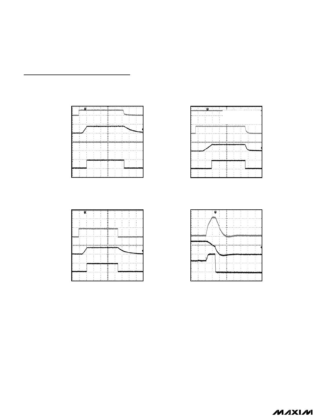
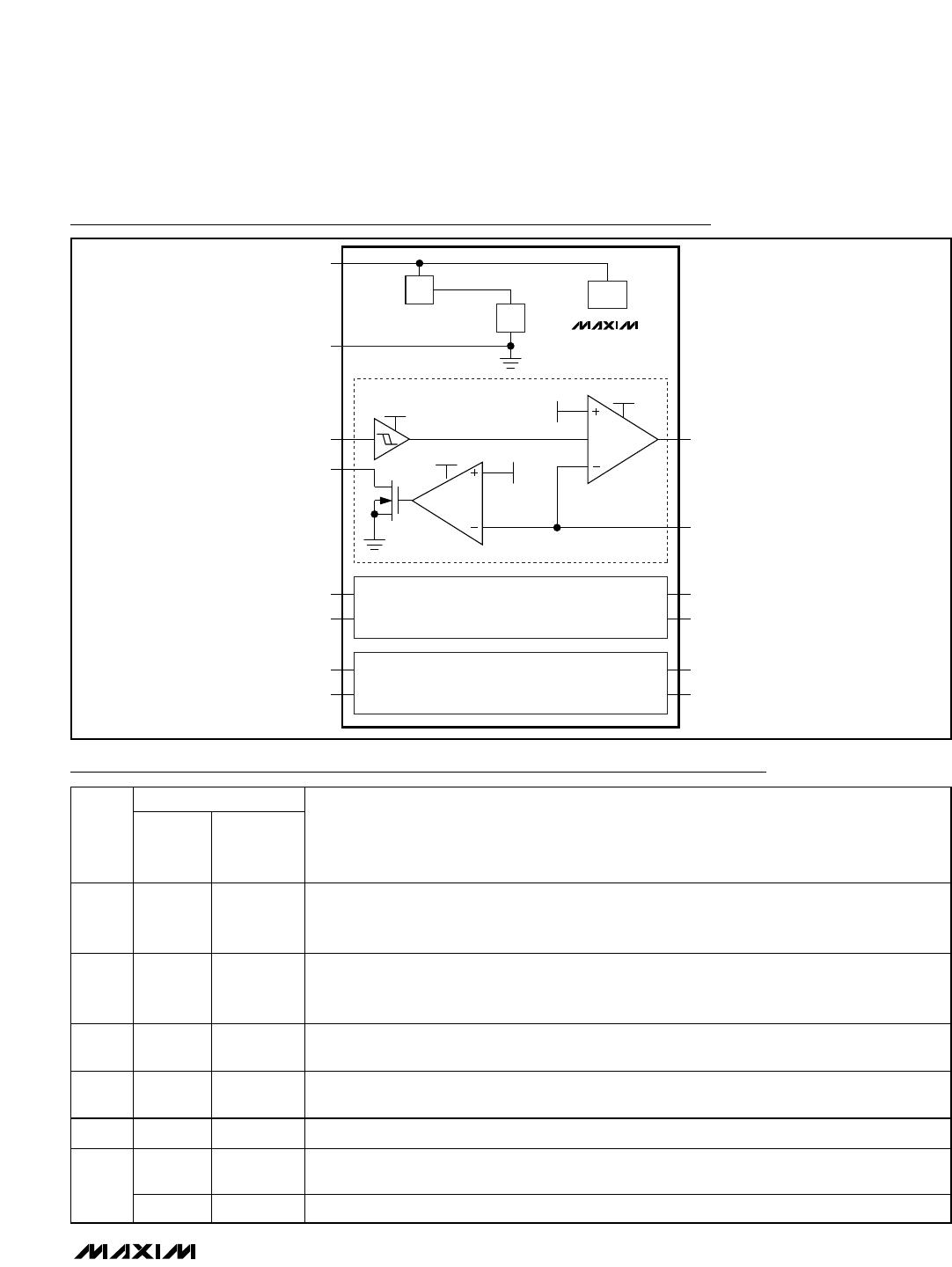
MAX8563/MAX8564/MAX8564A
±1%, Ultra-Low Output Voltage, Dual and Triple
Linear n-FET Controllers
4 _______________________________________________________________________________________
Typical Operating Characteristics (continued)
(Circuit of Figure 1, T
A
= +25°C.)
POWER-ON SEQUENCING WITH V
DD
MAX8563 toc07
V
DD
V
POK1
V
IN1
V
OUT1
2V/div
2V/div
2V/div
20V/div
20ms/div
0
0
0
0
POWER-ON SEQUENCING WITH V
IN
MAX8563 toc08
V
DD
V
POK1
V
OUT1
V
IN1
2V/div
2V/div
2V/div
20V/div
10ms/div
0
0
0
0
ENABLE CONFIGURED AS
SHOWN IN FIGURE 4
RD = 100kΩ, RE = 4kΩ
ENABLE-ON SEQUENCING
MAX8563 toc09
V
IN1
V
POK1
V
OUT1
EN1
2V/div
2V/div
2V/div
2V/div
20ms/div
0
0
0
0
SHORT-CIRCUIT PROTECTION
MAX8563 toc10
I
OUT1
V
DRV1
V
OUT1
5A/div
2V/div
1V/div
20μs/div
0
0
0
MAX8563/MAX8564/MAX8564A
±1%, Ultra-Low Output Voltage, Dual and Triple
Linear n-FET Controllers
_______________________________________________________________________________________ 5
V
DD
V
DD
VL
0.5V
POK
COMPARATOR
GM
LDO
CONTROLLER 1
LDO
CONTROLLER 2
LDO
CONTROLLER 3
0.5V
REF
VL
UVLO
V
DD
EN1
POK1
GND
EN2
POK2
EN3
POK3 FB3
DRV3
DRV2
FB1
FB2
DRV1
MAX8563
MAX8564
MAX8564A
Functional Diagram
Pin Description
NAME
PIN
MAX8563
MAX8564/
MAX8564A
FUNCTION
1 DRV1 DRV1
Output n-MOSFET Drive. Drives the gate of an external n-channel MOSFET to regulate output 1.
DRV1 is internally pulled to ground when EN1 is logic low. Connect an external series RC circuit
for compensation. See the Stability Compensation section.
2FB1 FB1
Feed b ack Inp ut for Outp ut 1. C onnect to the center of a r esi stor - d i vi d er b etw een outp ut 1 and GN D to
set the outp ut vol tag e of outp ut 1. The feed b ack r eg ul ati on vol tag e i s 0.500V . S ee the Outp ut V ol tag e
S etti ng secti on.
3 EN1 EN1
Enable Control for Output 1. Drive logic high to enable output 1, or logic low to disable the
output. Connect to V
DD
for always-on operation.
4 POK1 POK1
Output 1 Power-Good Signal. Open-drain output pulls low when output 1 is 12% below the
nominal regulated voltage.
5 GND GND Ground
POK2
Output 2 Power-Good Signal. Open-drain output pulls low when output 2 is 12% below the
nominal regulated voltage.
6
N.C. No Internal Connection
MAX8563/MAX8564/MAX8564A
±1%, Ultra-Low Output Voltage, Dual and Triple
Linear n-FET Controllers
6 _______________________________________________________________________________________
Pin Description (continued)
NAME
MAX8563
MAX8564/
MAX8564A
FUNCTION
EN2
Enable Control for Output 2. Drive logic high to enable output 2, or logic low to disable the
output. Connect to V
DD
for always-on operation.
7
DRV3
O utp ut 3 n- M O S FE T D r i ve. D r i ves the g ate of an exter nal n- channel M O S FE T to r eg ul ate outp ut 3.
DRV3 is internally pulled to ground when EN3 is logic low. Connect an external series RC circuit
for compensation. See the Stability Compensation section.
FB2
Feedback Input for Output 2. Connect to the center of a resistor-divider between output 2 and
GND to set the output voltage of output 2. The feedback regulation voltage is 0.500V. See the
Output Voltage Setting section.
8
FB3
Feedback Input for Output 3. Connect to the center of a resistor-divider between output 3 and
GND to set the output voltage of output 3. The feedback regulation voltage is 0.500V. See the
Output Voltage Setting section.
DRV2
O utp ut 2 n- M O S FE T D r i ve. D r i ves the g ate of the exter nal n- channel M OS FE T to r eg ul ate outp ut 2.
DRV2 is internally pulled to ground when EN2 is logic low. Connect an external series RC circuit
for compensation. See the Stability Compensation section.
9
EN3
Enable Control for Output 3. Drive logic high to enable output 3, or logic low to disable the
output. Connect to V
DD
for always-on operation.
—V
DD
+5V or +12V Supply Input. Connect to external +5V or +12V supply rail. Bypass with a 0.1µF
ceramic or larger capacitor.
10
POK3
Output 3 Power-Good Signal. Open-drain output pulls low when output 3 is 12% below the
nominal regulated voltage.
11 N.C. No Internal Connection
12 POK2
Output 2 Power-Good Signal. Open-drain output pulls low when output 2 is 12% below the
nominal regulated voltage.
13 EN2
Enable Control for Output 2. Drive logic high to enable output 2, or logic low to disable the
output. Connect to a V
DD
for always-on operation.
14 FB2
Feedback Input for Output 2. Connect to the center of a resistor-divider between output 2 and
GND to set the output voltage of output 2. The feedback regulation voltage is 0.500V. See the
Output Voltage Setting section.
15 DRV2
O utp ut 2 n- M O S FE T D r i ve. D r i ves the g ate of the exter nal n- channel M OS FE T to r eg ul ate outp ut 2.
DRV2 is internally pulled to ground when EN2 is logic low. Connect an external series RC circuit
for compensation. See the Stability Compensation section.
16 V
DD
+5V or +12V Supply Input. Connect to an external +5V or +12V supply rail. Bypass with a 0.1µF
ceramic or larger capacitor.

MAX8564AEUB+

Mfr. #:
Manufacturer:
Maxim Integrated
Description:
LDO Voltage Controllers Dual & Triple Linear n-FET Controller
Lifecycle:
New from this manufacturer.
Delivery:
DHL FedEx Ups TNT EMS
Payment:
T/T Paypal Visa MoneyGram Western Union