MAX8563/MAX8564/MAX8564A
Set R
D
= 100kΩ. The above equations also assume that
V
DD
> V
IN_
> 1V when V
IN_
is on or at a high-voltage
state, and that V
DD
> 3V.
Example: Connect 100kΩ from EN to V
DD
and 4kΩ from
EN_ to IN_. Thus, when V
DD
= 12V and V
IN
_ = 0V, then
V
EN
_ = 0.46V. When V
DD
= 12V and V
IN
_ = 1.2V, then
V
EN
_ = 1.6V.
Alternately, to avoid fault shutdown due to the delay of
V
IN
relative to V
DD
, pull EN_ low with a separate control
logic and only drive high when V
IN
reaches a steady-
state value.
Output Voltage
The output voltage range at the source of the n-MOSFET
is from 0.5V to 3.3V when V
DD
is 12V and from 0.5V to
1.8V when V
DD
is 5V. The maximum output voltage is a
function of the minimum gate-to-source voltage (V
GS
) of
the MOSFET and V
DD
.
The external n-MOSFET contains a parasitic diode from
source to drain. If the output is ever anticipated to
exceed the input, current flows from source to drain. If
this is undesirable, external protection is needed. A
simple solution is the placement of a diode in series,
from IN_ to the drain of the n-MOSFET, so that reverse
current is not possible. Due to the forward-voltage drop
of the diode, the maximum output voltage is reduced
and additional power is consumed in the diode.
Enable and POK
The MAX8563/MAX8564/MAX8564A have independent
enable control inputs (EN1, EN2, and EN3). Drive EN1
high to enable output 1. Drive EN2 high to enable out-
put 2. Drive EN3 high to enable output 3. When EN_ is
driven low, the corresponding DRV_ is internally pulled
to GND and POK_ is internally pulled low.
The POK_ is an open-drain output that provides the sta-
tus of the output voltage and pulls low depending upon
circuit conditions. During startup, once the FB_ reaches
the POK_ threshold, the POK_ signal goes high. The
POK_ threshold has 30mV of hysteresis. When the out-
put voltage drops 12% below the nominal regulated
voltage, POK_ pulls low. All POK_ outputs pull low
when UVLO is activated or when the internal VL regula-
tor and reference are not ready.
Output Undervoltage and
Overload Protection
When an overload event or short circuit occurs, the
device that is most vulnerable is the external n-MOSFET.
The MAX8563/MAX8564/MAX8564A monitor the output
voltage to protect the MOSFET. When DRV_ is at its maxi-
mum voltage and the output voltage drops below 80%
but is still greater than 60% of its nominal voltage for
more than 50µs, the MAX8563/MAX8564/MAX8564A
shut down that particular regulator output by pulling
DRV_ to GND. Note that there is an additional inherent
delay in turning off the MOSFET. The delay is a function
of the compensation capacitor and the MOSFET. If the
output recovers to greater than 80% within 50µs, it is not
considered to be in overload and no action is taken.
When the output voltage drops below 60% of its nominal
voltage, the MAX8563/MAX8564/MAX8564A immediately
shut down that particular regulator output by pulling
DRV_ to GND. To restart that particular LDO, V
DD
must
be recycled below the UVLO or the corresponding EN_
must be recycled. The overload protection is shown in
the Typical Operating Characteristics.
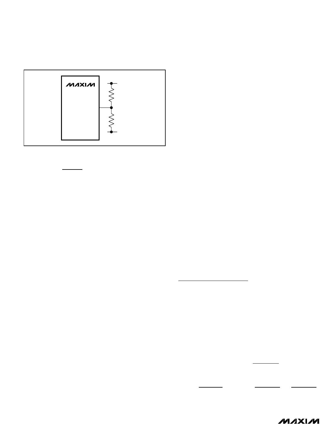
Design Procedure
Output Voltage Setting
The minimum output voltage for each controller of the
MAX8563/MAX8564/MAX8564A is typically 0.5V. The
maximum output voltage is adjustable up to 3.3V with
V
DD
= 12V, and up to 1.8V with V
DD
= 5V. To set the out-
put voltage, connect the FB_ pin to the center of a volt-
age-divider between OUT_ and GND (Figure 5). The
resistor-divider current should be at least 1mA per 1A of
maximum output current; i.e., for a 3A maximum output
current, set the resistor-divider bias current to 3mA:
R
V
I
V
II
B
FB
OUT MIN
FB
OUT MAX OUT MAX
() () ()
≤=× =1000
500
I
I
OUT MIN
OUT MAX
()
()
1000
13.
__
<
+
×
()
+
R
RR
VV V
E
ED
DD IN IN
±1%, Ultra-Low Output Voltage, Dual and Triple
Linear n-FET Controllers
10 ______________________________________________________________________________________
MAX8563
MAX8564
MAX8564A
EN_
V
DD
IN_
R
D
R
E
Figure 4. Voltage-Divider on EN_
To set the output voltage to 0.5V, disconnect R
B
from
FB_ and connect it to OUT_; this change maintains the
minimum load requirement on the output. In this case,
R
A
can vary from 1kΩ to 10kΩ.
Input and Output Capacitor Selection
The input filter capacitor aids in providing low input
impedance to the regulator and also reduces peak cur-
rents drawn from the power source during transient
conditions. Use a minimum 2.2µF ceramic capacitor
from IN_ (drain of the external pass n-MOSFET) to GND
(see Figures 1 and 2). If large line transients or load
transients are expected, increase the input capaci-
tance to help minimize output voltage changes.
The output filter capacitor and its equivalent series
resistance (ESR) contribute to the stability of the regula-
tor (see the Stability Compensation section) and affect
the load-transient response. If large step loads (no load
to full load) are expected, and a very fast response
(less than a few microseconds) is required, use a
100µF, 18mΩ POSCAP for the output capacitor. If a
larger capacitance is desired, keep the capacitance
ESR product (C
OUT
x R
ESR
) in the 1µs to 5µs range.
If the application expects smaller load steps (less than
50% of full load), then use a 6.8µF ceramic capacitor or
larger per ampere of maximum output current. This
option reduces the size and cost of the regulator circuit.
Note that some ceramic dielectrics exhibit large capaci-
tance variation with temperature. Use X7R or X5R
dielectrics to ensure sufficient capacitance at all operat-
ing temperatures. Tantalum and aluminum capacitors
are not recommended.
Power MOSFET Selection
The MAX8563/MAX8564/MAX8564A use an n-channel
MOSFET as the series pass transistor instead of a p-
channel MOSFET to reduce cost. The selected MOS-
FET must have a gate threshold voltage that meets the
following criteria:
V
GS_MAX
V
DD
- V
OUT_
where V
DD
is the controller bias voltage, and V
GS_MAX
is the maximum gate voltage required to yield the on-
resistance (R
DS_ON
) specified by the manufacturer’s
data sheet. R
DS_ON
multiplied by the maximum output
current (load current) is the maximum voltage dropout
across the MOSFET, V
DS
_
MIN
. Make sure that V
DS
_
MIN
meets the condition below to avoid entering dropout,
where output voltage starts to decrease and any ripple
on the input also passes through to the output:
V
IN_MIN
> V
DS
_
MIN
+ V
OUT
where V
IN_MIN
is the minimum input voltage at the drain
of the MOSFET. V
DS
_
MIN
has a positive temperature
coefficient; therefore, the value of V
DS
_
MIN
at the highest
operating junction temperature should be used.
For thermal management, the maximum power dissipa-
tion in the MOSFET is calculated by:
P
D
= (V
IN_MAX
- V
OUT
) x I
OUT_MAX
The MOSFET is typically in an SMT package. Refer to
the MOSFET data sheet for the PC board area needed
to meet the maximum operating junction temperature
required.
Stability Compensation
Connect a resistor, R
C
, and a capacitor, C
C
, in series
from the DRV_ pin to GND. The values of the compen-
sation network depend upon the external MOSFET
characteristics, the output current range, and the pro-
grammed output voltage. The following parameters are
needed from the MOSFET data sheet: the input capaci-
tance (C
ISS
at V
DS
= 1V), the typical forward transcon-
ductance (g
FS
), and the current at which g
FS
was
measured (I
DFS
). Calculate the transconductance of
the FET at the maximum load current (I
OUT_MAX
):
gg
I
I
C MAX FS
OUT MAX
DFS
()
_
RR
V
V
RV
AB
OUT
FB
B OUT
×
()
−−12 1
MAX8563/MAX8564/MAX8564A
±1%, Ultra-Low Output Voltage, Dual and Triple
Linear n-FET Controllers
______________________________________________________________________________________ 11
MAX8563
MAX8564
MAX8564A
FB_
OUT_
R
A
R
B
Figure 5. Adjustable Output Voltage
MAX8563/MAX8564/MAX8564A
For the best transient response in applications with
large step loads (see the Input and Output Capacitor
Selection section for output capacitance requirements),
use the following equations to select the compensation
components:
where C
OUT
is the output capacitance and R
ESR
is the
ESR of C
OUT
.
To use a low-cost ceramic capacitor (see the Input and
Output Capacitor Selection section for load-transient
response characteristics), use the following equations
to select the compensation components:
Example
OUTPUT 1 of Figure 1 is used in this example. Table 1
shows the values required to calculate the compensa-
tion. The values were taken from the appropriate data
sheets and Figure 1.
PC Board Layout Guidelines
Due to the high-current paths and tight output accuracy
required by most applications, careful PC board layout is
required. An evaluation kit (MAX8563EVKIT) is available
to speed design.
It is important to keep all traces as short as possible to
maximize the high-current trace dimensions to reduce the
effect of undesirable parasitic inductance. The MOSFET
dissipates a fair amount of heat due to the high currents
involved, especially during large input-to-output voltage
differences. To dissipate the heat generated by the
MOSFET, make power traces very wide with a large
amount of copper area. An efficient way to achieve good
power dissipation on a surface-mount package is to lay
out copper areas directly under the MOSFET package on
multiple layers and connect the areas through vias. Use a
ground plane to minimize impedance and inductance. In
addition to the usual high-power considerations, here are
four tips to ensure high output accuracy:
Ensure that the feedback connection to C
OUT_
is
short and direct.
Place the feedback resistors next to the FB pin.
Place R
C
and C
C
next to the DRV_ pin.
Ensure FB_ and DRV_ traces are away from noisy
sources to ensure tight accuracy.
gSx
A
A
S
Cx
Vx Fx Sx
Sx
m
Sx V A
pF F use F
C MAX
C
()
.
.
.
.
. .
.
. . .
., .
==
=
+
+
()
=
30
15
88
12 4
016
1 5 100 12 4
12 4
18 1
12 4 1 5 1 5
2500 0 90 1
2
μ
μμ
Ω
RRx
Vx Fx Sx m
FSxV A
use
C
. .
. . .
. , .
=
+
()
+
()
=
59
1 5 100 12 4 18 1
1 124 15 15
599 4 620
μ
μ
Ω
ΩΩ
C
Cxg
gxVI
C
Rx
C
Cxg
C
OUT C MAX
C MAX OUT OUT MAX
ISS
C
OUT
C C MAX
()
() _
()
=
+
()
=
15
C
VC
ggR
gVI
C
R
VxCg xR
Cxg V I
C
OUT OUT
C MAX C MAX ESR
C MAX OUT OUT MAX
ISS
C
OUT OUT C MAX ESR
C C MAX OUT OUT
.
() ()
() _
()
() _
=
×× ×
××+
()
×+
()
+
()
×+
016
1
59
1
2
MAXMAX
()
±1%, Ultra-Low Output Voltage, Dual and Triple
Linear n-FET Controllers
12 ______________________________________________________________________________________
Table 1. Parameters Required to
Calculate Compensation
PARAMETER
CONDITIONS
VALUE UNITS
MOSFET C
ISS
V
DS
= 1V 2500 pF
MOSFET GFS
IDFS = 8.8A
30 S
V
OUT1
Figure 1 1.5 V
I
OUT_MAX
Figure 1 1.5 A
C
OUT1
Figure 1 100 µF
R
ESR
Figure 1 18 mΩ

MAX8564AEUB+

Mfr. #:
Manufacturer:
Maxim Integrated
Description:
LDO Voltage Controllers Dual & Triple Linear n-FET Controller
Lifecycle:
New from this manufacturer.
Delivery:
DHL FedEx Ups TNT EMS
Payment:
T/T Paypal Visa MoneyGram Western Union