LTC2482
10
2482fc
TIMING DIAGRAMS
Timing Diagram Using Internal SCK
SDO
SCK
t
1
t
3
SLEEP
t
KQMAX
CONVERSIONDATA OUT
t
KQMIN
t
2
2482 TD1
CS
Timing Diagram Using External SCK
SDO
SCK
t
1
t
5
t
6
t
4
SLEEP
t
KQMAX
CONVERSIONDATA OUT
t
KQMIN
t
2
2482 TD2
CS
APPLICATIONS INFORMATION
CONVERTER OPERATION
Converter Operation Cycle
The LTC2482 is a low power, delta-sigma analog-to-digital
converter with an easy-to-use 3-wire serial interface and
automatic differential input current cancellation. Its opera-
tion is made up of three states. The converter operating
cycle begins with the conversion, followed by the low power
sleep state and ends with the data output (see Figure 1).
The 3-wire interface consists of serial data output (SDO),
serial clock (SCK) and chip select (CS).
Initially, the LTC2482 performs a conversion. Once the
conversion is complete, the device enters the sleep state.
While in this sleep state, power consumption is reduced
CONVERT
SLEEP
DATA OUTPUT
2482 F01
TRUE
FALSE
CS = LOW
AND
SCK
Figure 1. LTC2482 State Transition Diagram
LTC2482
11
2482fc
APPLICATIONS INFORMATION
by two orders of magnitude. The part remains in the sleep
state as long as CS is high. The conversion result is held
indefi nitely in a static shift register while the converter is
in the sleep state.
Once CS is pulled low, the device exits the low power mode
and enters the data output state. If CS is pulled high before
the fi rst rising edge of SCK, the device returns to the low
power sleep mode and the conversion result is still held
in the internal static shift register. If CS remains low after
the fi rst rising edge of SCK, the device begins outputting
the conversion result. Taking CS high at this point will
terminate the data output state and start a new conversion.
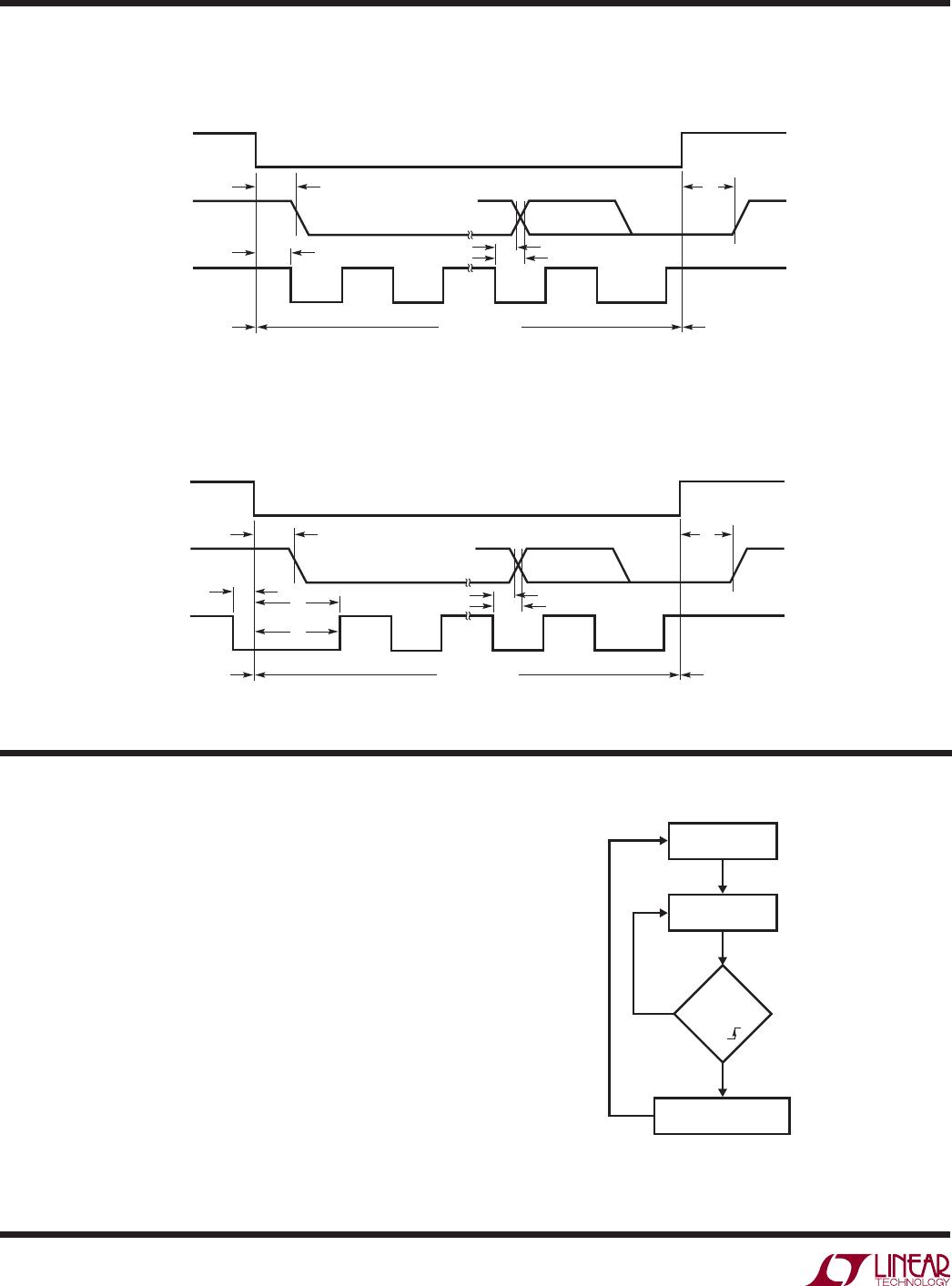
The conversion result is shifted out of the device through
the serial data output pin (SDO) on the falling edge of the
serial clock (SCK) (see Figure 2).
Through timing control of the CS and SCK pins, the LTC2482
offers several fl exible modes of operation (internal or
external SCK and free-running conversion modes). These
various modes do not require programming confi guration
registers; moreover, they do not disturb the cyclic operation
described above. These modes of operation are described
in detail in the Serial Interface Timing Modes section.
Easy Drive Input Current Cancellation
The LTC2482 combines a high precision delta-sigma ADC
with an automatic differential input current cancellation
front end. A proprietary front-end passive sampling net-
work transparently removes the differential input current.
This enables external RC networks and high impedance
sensors to directly interface to the LTC2482 without
external amplifi ers. The remaining common mode input
current is eliminated by either balancing the differential
input impedances or setting the common mode input
equal to the common mode reference (see Automatic Input
Current Cancellation section). This unique architecture
does not require on-chip buffers enabling input signals to
swing all the way to ground and up to V
CC
. Furthermore,
the cancellation does not interfere with the transparent
offset and full-scale autocalibration and the absolute ac-
curacy (full scale + offset + linearity) is maintained with
external RC networks.
Output Data Format
The LTC2482 serial output data stream is 24 bits long. The
rst 3 bits represent status information indicating the sign
and conversion state. The next 17 bits are the conversion
result, MSB fi rst. The remaining 4 bits are always zero.
Bit 21 and Bit 20 together are also used to indicate an
underrange condition (the differential input voltage is
below –FS) or an overrange condition (the differential
input voltage is above +FS).
In applications where a processor generates 32 clock
cycles, or to remain compatible with higher resolution
converters, the LTC2482’s digital interface will ignore
extra clock edges seen during the next conversion period
after the 24th and output “1” for the extra clock cycles.
Furthermore, CS may be pulled high prior to outputting
all 24 bits, aborting the data out transfer and initiating a
new conversion.
CS
SDO
Hi-Z
SIG
BIT 21 BIT 20 BIT 19 BIT 18 BIT 4 BIT 3 BIT 2 BIT 1 BIT 0BIT 22BIT 23
DMY MSB B16
CONVERSION RESULT
LSB
SCK
SLEEP DATA OUTPUT
EOC
CONVERSION
2482 F02
Figure 2. Output Data Timing
LTC2482
12
2482fc
APPLICATIONS INFORMATION
Bit 23 (fi rst output bit) is the end of conversion (EOC)
indicator. This bit is available at the SDO pin during the
conversion and sleep states whenever the CS pin is low.
This bit is high during the conversion and goes low when
the conversion is complete.
Bit 22 (second output bit) is a dummy bit (DMY) and is
always low.
Bit 21 (third output bit) is the conversion result sign
indicator (SIG). If V
IN
is >0, this bit is high. If V
IN
is <0,
this bit is low.
Bit 20 (fourth output bit) is the most signifi cant bit (MSB)
of the result. This bit in conjunction with Bit 21 also
provides the underrange or overrange indication. If both
Bit 21 and Bit 20 are high, the differential input voltage is
above +FS. If both Bit 21 and Bit 20 are low, the differential
input voltage is below –FS.
The function of these bits is summarized in Table 1.
Table 1. LTC2482 Status Bits
INPUT RANGE
BIT 23
EOC
BIT 22
DMY
BIT 21
SIG
BIT 20
MSB
V
IN
≥ 0.5 • V
REF
0011
0V ≤ V
IN
< 0.5 • V
REF
0010
–0.5 • V
REF
≤ V
IN
< 0V 0001
V
IN
< –0.5 • V
REF
0000
Bits 20-4 are the 16-bit plus sign conversion result MSB
rst.
Bits 3-0 are always low and are included to maintain
software compatibility with the LTC2480.
Data is shifted out of the SDO pin under control of the
serial clock (SCK) (see Figure 2). Whenever CS is high,
SDO remains high impedance and any externally gener-
ated SCK clock pulses are ignored by the internal data
out shift register.
In order to shift the conversion result out of the device,
CS must fi rst be driven low. EOC is seen at the SDO pin
of the device once CS is pulled low. EOC changes in real
time from high to low at the completion of a conversion.
This signal may be used as an interrupt for an external
microcontroller. Bit 23 (EOC) can be captured on the fi rst
rising edge of SCK. Bit 22 is shifted out of the device on
the fi rst falling edge of SCK. The fi nal data bit (Bit 0) is
shifted out on the falling edge of the 23rd SCK and may
be latched on the rising edge of the 24th SCK pulse. On
the falling edge of the 24th SCK pulse, SDO goes high
indicating the initiation of a new conversion cycle. This
bit serves as EOC (Bit 23) for the next conversion cycle.
Table 2 summarizes the output data format.
As long as the voltage on the IN
+
and IN
pins is main-
tained within the –0.3V to (V
CC
+ 0.3V) absolute maximum
operating range, a conversion result is generated for any
differential input voltage V
IN
from –FS = –0.5 • V
REF
to
+FS = 0.5 • V
REF
. For differential input voltages greater
than +FS, the conversion result is clamped to the value
corresponding to the +FS + 1LSB. For differential input
voltages below –FS, the conversion result is clamped to
the value corresponding to –FS – 1LSB.
Table 2. LTC2482 Output Data Format
DIFFERENTIAL INPUT VOLTAGE
V
IN
*
BIT 23
EOC
BIT 22
DMY
BIT 21
SIG
BIT 20
MSB BIT 19 BIT 18 BIT 17 BIT 4 BITS 3-0
V
IN
* FS** 001100000
FS** 1LSB 001011110
0.5 • FS** 001010000
0.5 • FS** – 1LSB 001001110
0 001000000
–1LSB 000111110
–0.5 • FS** 000110000
–0.5 • FS** – 1LSB 000101110
FS** 000100000
V
IN
* <FS** 000011110
*The differential input voltage V
IN
= IN
+
– IN
. **The full-scale voltage FS = 0.5 • V
REF
.

LTC2482CDD#TRPBF

Mfr. #:
Manufacturer:
Analog Devices Inc.
Description:
Analog to Digital Converters - ADC 16-Bit Delta Sigma ADC
Lifecycle:
New from this manufacturer.
Delivery:
DHL FedEx Ups TNT EMS
Payment:
T/T Paypal Visa MoneyGram Western Union