MT89L86 Data Sheet
40
Zarlink Semiconductor Inc.
† Timing is over recommended temperature & power supply voltages.
‡ Typical figures are at 25
C and are for design aid only: not guaranteed and not subject to production testing.
* High Impedance is measured by pulling to the appropriate rail with R
L
, with timing corrected to cancel time taken to discharge C
L
.
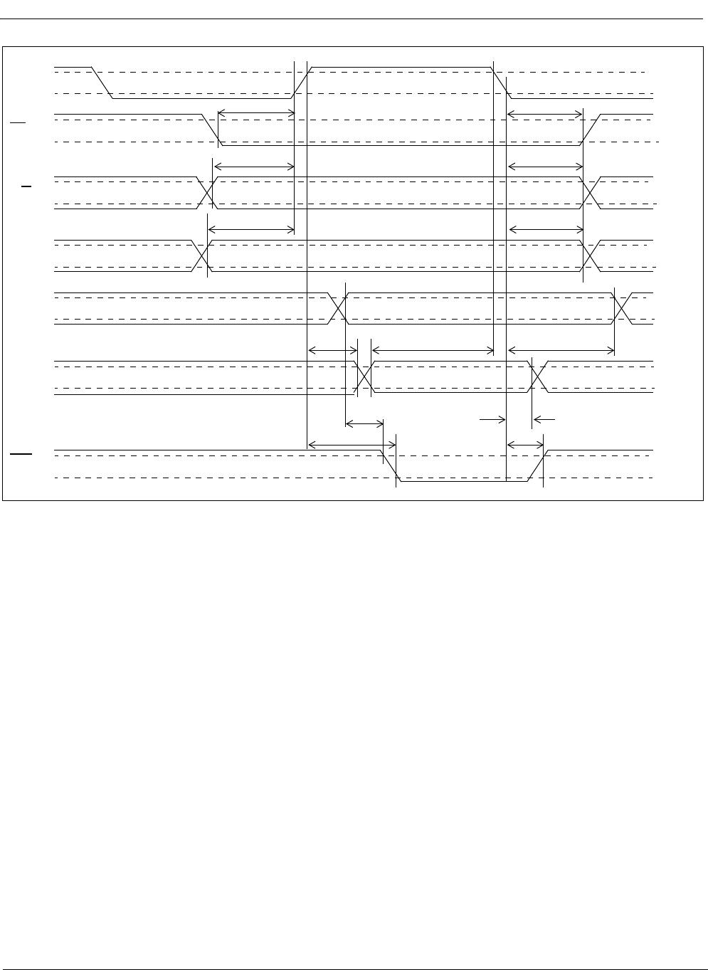
AC Electrical Characteristics
†
- Motorola Non-Multiplexed Bus Mode
Voltages are with respect to ground (VSS) unless otherwise stated.
Characteristics Sym. Min. Typ.
‡
Max. Units Test Conditions
1CS
Setup from DS rising t
CSS
0ns
2R/W
Setup from DS rising t
RWS
5ns
3 Add setup from DS rising t
ADS
5ns
4CS
hold after DS falling t
CSH
0ns
5R/W
hold after DS falling t
RWH
5ns
6 Add hold after DS falling t
ADH
8ns
7 Data setup from DTA
Low on Read t
DDR
0ns
C
L
=150 pF
8 Data hold on read
t
DHR
10 50 90 ns C
L
=150 pF,
R
L
=1 K
9 Data setup on write (fast write) t
DSW
0ns
10 Valid Data Delay on write
(slow write)
t
SWD
122 ns
11 Data hold on write t
DHW
5ns
12 Acknowledgment Delay:
Reading Data Memory
Reading/Writing Conn. Memories
Writing Control & Mode Regs.
Reading from Control & Mode Regs.
t
AKD
560
62/30
25
52
1220
120/53
65
120
ns
ns
ns
ns
C
L
=150 pF
13 Acknowledgment Hold Time t
AKH
50 80 ns C
L
=150 pF,
R
L
=1 K