MT89L86 Data Sheet
3
Zarlink Semiconductor Inc.
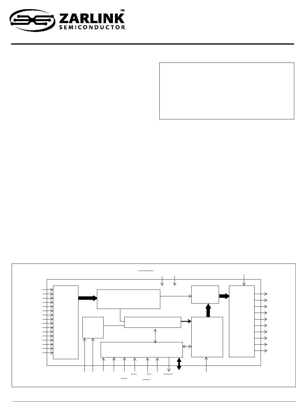
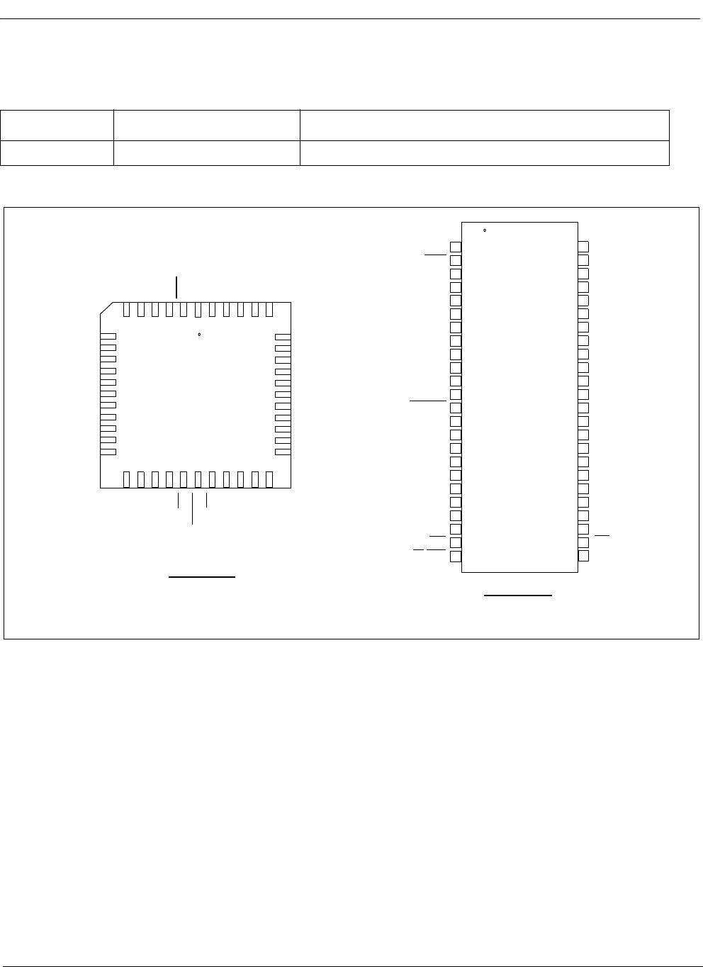
Pin Description
Pin #
Name Description
44
PLCC
48
SSOP
22 DTA
Data Acknowledgment (Open Drain Output). This active low output indicates that a
data bus transfer is complete. A pull-up resistor is required at this output.
3-5
7-9
3-5
7-9
STi0-5 ST-BUS Inputs 0 to 5 (5 V tolerant Inputs). Serial data input streams. These streams
may have data rates of 2.048, 4.096 or 8.192 Mbit/s with 32, 64 or 128 channels,
respectively.
10 10 STi6/A6 ST-BUS Input 6/Addr.6 input (5 V tolerant Input). The function of this pin is
determined by the switching configuration enabled. If non-multiplexed CPU bus is used
along with a higher input rate of 8.192 or 4.096 Mb/s, this pin provides A6 address
input function. For 2.048 and 4.096 Mb/s (8x4) applications or when the multiplexed
CPU bus interface is selected, this pin assumes STi6 function. See Control Register
bits description and Tables 1, 2, 6 & 7 for more details.
Note that for applications where both A6 and STi6 inputs are required simultaneously
(e.g., 8 x 4 switching configuration at 4.096 Mb/s or rate conversion between
2.048 Mb/s to 4.196 or 8.192 Mb/s) the A6 input should be connected to pin STo6/A6.
11 11 STi7/A7 ST-BUS Input 7/Addr.7 input (5 V tolerant Input): The function of this pin is
determined by the switching configuration enabled. If non-multiplexed CPU bus is used
along with a higher input rate of 8.192 Mb/s, this pin provides A7 address input
function.
For 2.048 and 4.096 Mb/s (8x4) applications or when the multiplexed CPU bus is
selected, this pin assumes STi7 function. See Control Register bits description and
Tables 1, 2, 6 & 7 for more details.
Note that for applications where both A7 and STi7 inputs are required simultaneously
(e.g., 2.048 to 8.192 Mb/s rate conversion) the A7 input should be connected to pin
STo7/A7.
12 12,36 V
DD
+3.3 Volt Power Supply.
13 RESET
Device Reset (5 V tolerant input). This pin is only available for the 48-pin SSOP
package. In normal operation, This active low input puts the MT89L86 in its reset state.
It clears the internal counters and registers. All ST-BUS outputs are set to the high
impedance state. The RESET
pin must be held low for a minimum of 100nsec to reset
the device.
13 14 FR Frame Pulse (5 V tolerant Input). This input accepts and automatically identifies frame
synchronization signals formatted according to ST-BUS and GCI interface
specifications.
14 15 CLK Clock (5 V tolerant Input). Serial clock for shifting data in/out on the serial streams.
Depending on the serial interface speed selected by IMS (Interface Mode Select)
register, the clock at this pin can be 4.096 or 8.192 MHz.
15-17 16-18 STi8/A0,
STi9/A1,
STi10/A2
Address 0-2 / Input Streams 8-10 (5 V tolerant Input). When the non-multiplexed
CPU bus is selected, these lines provide the A0-A2 address lines to the MT89L86
internal registers. When the 16x8 switching configuration is selected, these pins are
ST-BUS serial inputs 8 to 10 receiving data at 2.048 Mb/s.
19-21 20-22 STi11/A3,
STi12/A4,
STi13/A5
Address 3-5 / Input Streams 11-13 (5 V tolerant Input). When the non-multiplexed
CPU bus is selected, these lines provide the A3-A5 address lines to the MT89L86
internal registers. When the 16x8 switching configuration is selected, these pins are
ST-BUS serial inputs 11 to 13 receiving data at 2.048 Mb/s.