MT89L86 Data Sheet
19
Zarlink Semiconductor Inc.
Figure 5 - Connection Memory High (CMH) Bits
x=Don’t care
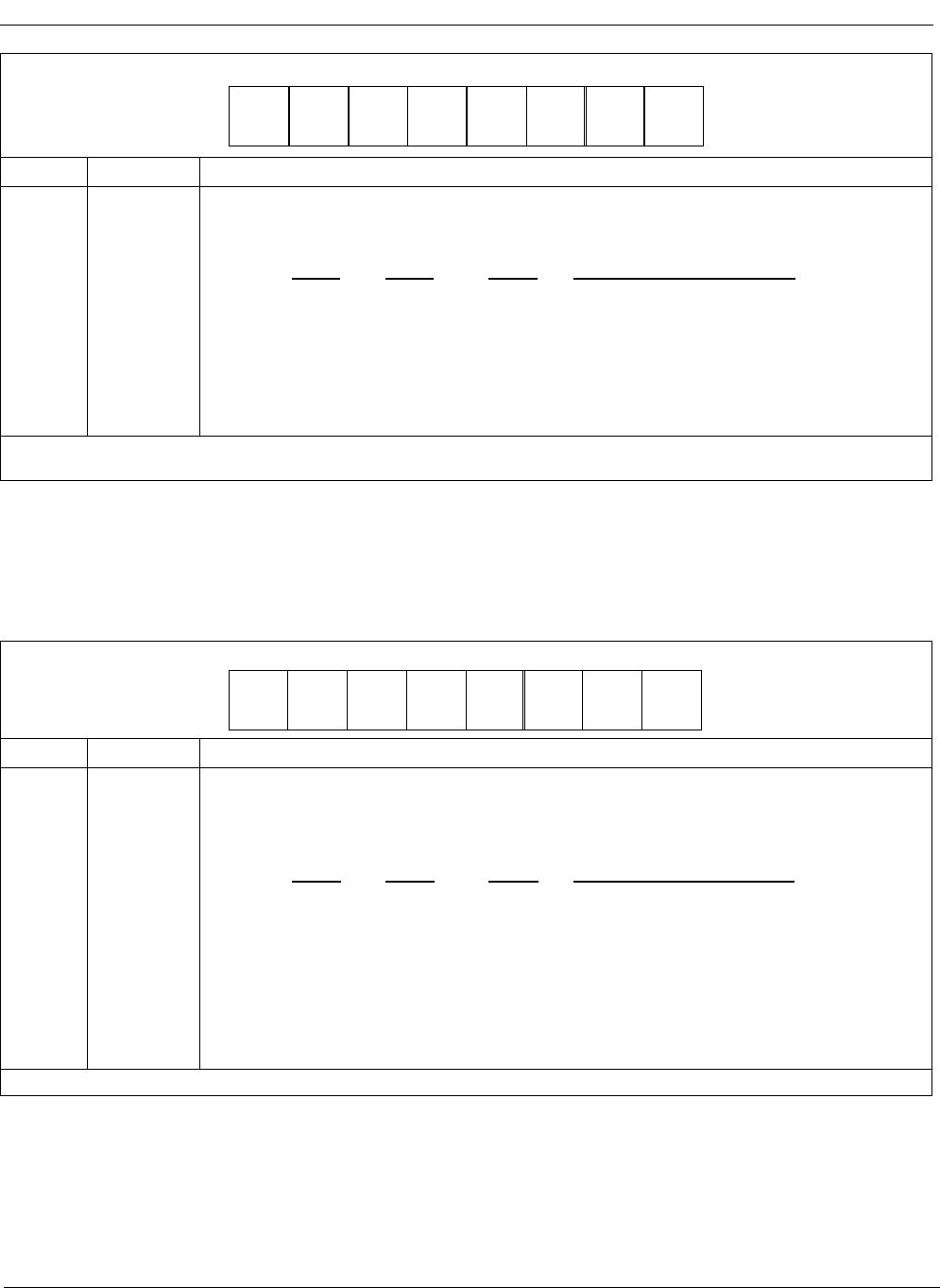
Connection Memory Low - Read/Write
Figure 6 - Connection Memory Low (CML) Bits
2 MC Message Channel. When 1, the contents of the corresponding location in Connection
Memory Low are output on the corresponding channel and stream. When 0, the contents
of the programmed location in Connection Memory Low act as an address for the Data
Memory and so determine the source of the connection to the location’s channel and
stream.
1 CSTo CSTo Bit. This bit is only available in 2.048 Mb/s applications. It drives a bit time on the
CSTo output pin.
0 OE Output Enable. This bit enables the output drivers on a per-channel basis. This allows
individual channels on individual streams to be made high-impedance, allowing switch
matrices to be constructed. A HIGH enables the driver and a LOW disables it.
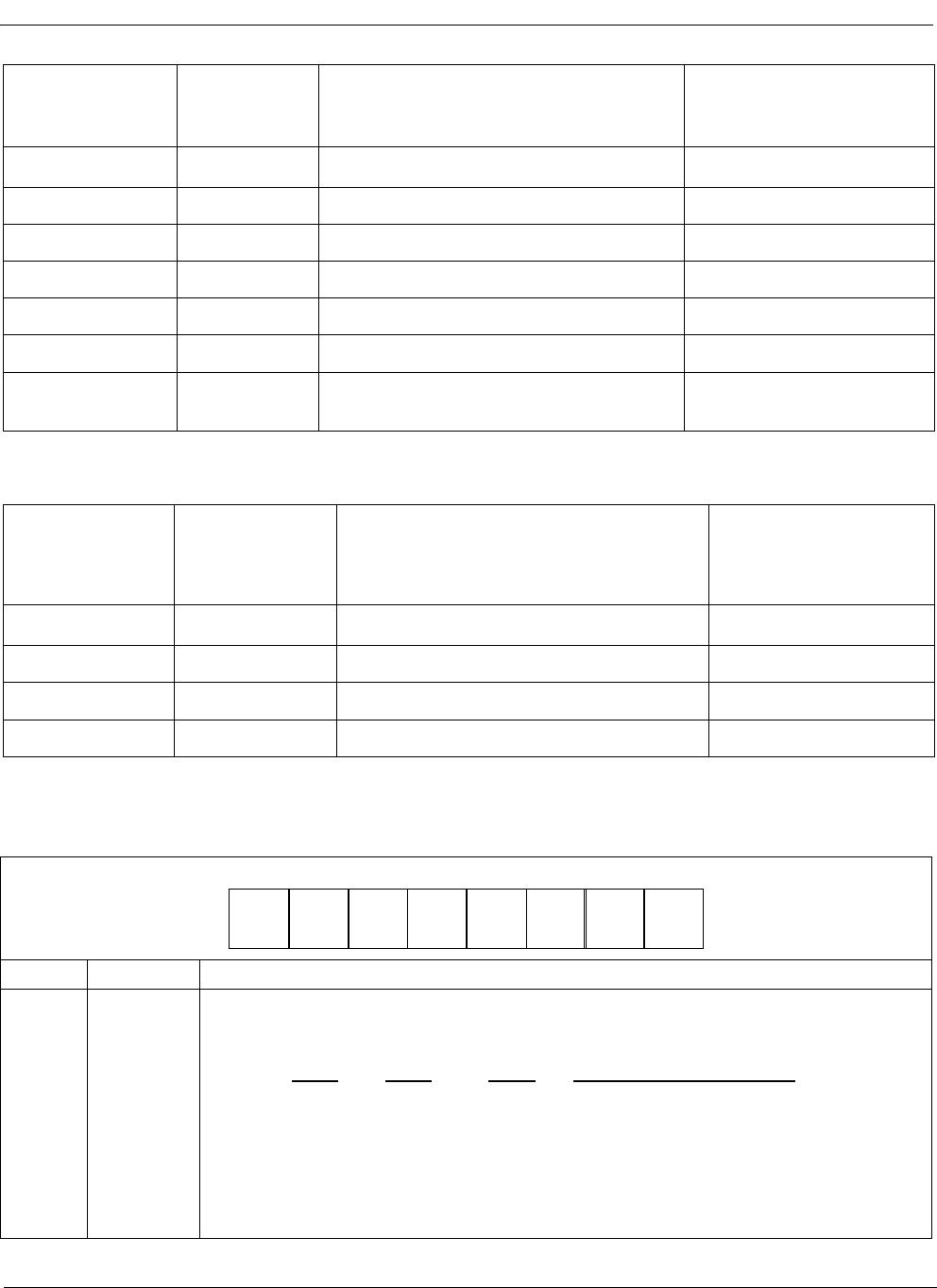
Bit Name Description
7-5 SAB2-0* Source Stream Address bits. These three bits are used together with SAB3 in CMH to
select up to 16 different source streams for the connection. Depending on the switching
configuration and the data rate selected in the application, 1, 2, 3 or all 4 SAB bits can be
used. See Tables 9 and 10 for details.
4-0 CAB4-0* Source Channel Address bits 0-4. These five bits are used together with CAB5-6 in
CMH to select up 128 different source channels for the connection. Depending on the
switching configuration and the data rate used in the application, 5, 6 or all 7 CAB bits
can be used to select respectively 32, 64 or 128 different channels.
See Tables 9 and 10 for details.
If bit two (MC) of the corresponding Connection High locations is 1, or if bit 6 of the Control Register is 1, then these entire eight bits are output
on the corresponding output channel and stream associated with this location. Otherwise, the bits are used as indicated to define the source
of the connection which is output on the channel and stream associated with this location.
Bit Name Description
XV/C SAB3 CAB6 CAB5 MC CSTo OE
76543210
(CM high bits)
SAB2 SAB1 SAB0 CAB4 CAB3 CAB2 CAB1 CAB0
76543210
(CM low bits)