MT89L86 Data Sheet
10
Zarlink Semiconductor Inc.
signals to be skewed at the input of the switch device. This may result in the system frame synchronization pulse to
be active at the MT89L86’s FR input before the first bit of the frame is received at the serial inputs.
When the input frame offset is enabled, an "internal delay" of up to four clock periods is added to the actual data
input sampling, providing the MT89L86 serial timing unit a new input frame reference. An internal virtual frame is
created which is aligned with the framing of the actual serial data coming in at the serial inputs and not with the FR
frame pulse input. In this operation, the transmission of the output frame on the serial links is still aligned to the
frame pulse input signal (FR).
The selection of the data input sampling delay is defined by the CPU in the Frame Input Offset Register (FIO). If this
function is not required in the user's applications, the FIO register should be set up during system initialization to a
state where offset functions are disabled.
Delay Through the MT89L86
The switching of information from the input serial streams to the output serial streams results in a delay. Depending
on the type of information to be switched, this MT89L86 can be programmed to perform time-slot interchange
functions with different throughput delay capabilities on a per-channel basis. For voice applications, variable
throughput delay can be selected ensuring minimum delay between input and output data. In wideband data
applications, constant throughput delay can be selected maintaining the frame integrity of the information through
the switch.
The delay through the device varies according to the type of throughput delay selected in the V
/C bit of the connect
memory high.
Variable Throughput Delay Mode (V
/C bit = 0)
Identical I/O Data Rates
The delay in this mode is dependent on the combination of source and destination channels and it is independent of
the input and output streams. The minimum delay achievable in this MT89L86 depends on the data rate selected
for the serial streams. For instance, for the 2.048 Mb/s data rate, the minimum delay achieved corresponds to three
time-slots. For the 4.096 Mb/s data rate it corresponds to five time-slots while it is nine time-slots for the 8.192 Mb/s
data rate. Switching configurations with input and output channels that provides more than its corresponding
minimum throughput delay, will have a throughput delay equal to the difference between the output and input
channels; i.e., the throughput delay will be less than one frame period. Table 3a shows the throughput delay for
each data rate operation.
Different I/O Data Rates
Except for the 2 Mb/s to 4 Mb/s and the 2 Mb/s to 8 Mb/s rate conversion operations, the throughput delay from the
MT89L86 may vary according to the output stream used for switching.
Table 3b explains the worst case conditions for the throughput delay when different I/O data rate switching
configurations are used.
Table 3a - Variable Throughput Delay Values for Identical I/O Rate Applications
n= input channel, t.s. = time-slot
Input Rate
Output Channel (# m)
m < n m=n, n+1, n+2 m= n+3, n+4 m=n+5, .. n+8 m > n+8
2.048 Mb/s 32-(n-m) t.s. m-n + 32 t.s. m-n t.s. m-n t.s. m-n t.s.
4.096 Mb/s 64-(n-m) t.s. m-n + 64 t.s. m-n+64 t.s. m-n t.s. m-n t.s.
8.192 Mb/s 128-(n-m) t.s. m-n + 128 t.s. m-n+128 t.s. m-n+128 t.s. m-n t.s.
MT89L86 Data Sheet
11
Zarlink Semiconductor Inc.
Table 3b - Min/Max Throughput Delay Values for Different I/O Rate Applications
Notes: dmin and dmax are measured in time-slots and at the point in time when the output channel is completely shifted out.
t.s. = time-slot
fr. = 125 s frame
2 Mb/s t.s. = 3.9 s
4 Mb/s t.s. = 1.95 s
8 Mb/s t.s. = 0.975 s
Constant Throughput Delay mode (V/C bit = 1)
In this mode frame sequence integrity is maintained in both Identical and Different I/O Data Rate operations by
making use of a multiple Data-Memory buffer technique. The input channels written in any of the buffers during
frame N will be read out during frame N+2. In applications at 2.048 Mb/s for instance, the minimum throughput
delay achievable in constant delay mode will be 32 time-slots; for example, when input time-slot 32 (channel 31) is
switched to output time-slot 1 (channel 0). Likewise, the maximum delay is achieved when the first time slot in a
frame (channel 0) is switched to the last time-slot in the frame (channel 31), resulting in 94 time-slots of delay.
To summarize, any input time-slot from input frame N will always be switched to the destination time-slot on
output frame N+2. Table 4 describes the constant throughput delay values at different data rates.
I/O Data Rate
Configuration
Output Stream Used
0, 1 2, 3 4, 5 6, 7
2 Mb/s to 4 Mb/s
dmin=5x 4Mb/s t.s.
dmax=1 fr.+(4x 4Mb/s t.s.)
2 Mb/s to 8 Mb/s
dmin=9x 8Mb/s t.s.
dmax=1 fr.+(8x 8Mb/s t.s.)
4 Mb/s to 2 Mb/s
dmin=3x 2Mb/s t.s.
dmax=1 fr.+(2x 2Mb/s t.s.)
dmin=(2x 2Mb/s t.s.)+(1x 4Mb/s t.s.)
dmax=1 fr.+(1x 2Mb/s t.s.)+(1x 4Mb/s t.s.)
8 Mb/s to 2 Mb/s
dmin=3x 2Mb/s t.s.
dmax=1 fr.+(2x 2Mb/s
t.s.)
dmin=(2x 2Mb/s t.s.)+
(3x 8Mb/s t.s.)
dmax=1 fr.+(1x 2Mb/s
t.s.)+(3x 8Mb/s t.s.)
dmin=(2x 2Mb/s t.s.)+
(2x 8Mb/s t.s.)
dmax=1 fr.+(1x 2Mb/s
t.s.)+(2x 8Mb/s t.s.)
dmin=(2x 2Mb/s t.s.)+
(1x 8Mb/s t.s.)
dmax=1 fr.+(1x 2Mb/s
t.s.)+(1x 8Mb/s t.s.)
MT89L86 Data Sheet
12
Zarlink Semiconductor Inc.
Table 4 - Constant Throughput Delay Values
Microprocessor Port
The non-multiplexed bus interface provided by the MT89L86 is identical to that provided in the MT8986 Digital
Switch device. In addition to the non-multiplexed bus, this 3.3 V MT89L86 device provides an enhanced
microprocessor interface with multiplexed bus structure compatible to both Motorola and Intel buses. The
multiplexed bus structure is selected by the CPU Interface Mode (IM) input pin.
If the IM input pin is connected to ground, the MT89L86’s parallel port assumes its default Motorola non-multiplexed
bus mode identical to that of MT8986. If the IM input is connected HIGH, the internal parallel microprocessor port
provides compatibility to MOTEL (MOtorola and InTEL compatible bus) interface allowing direct connection to Intel,
National and Motorola CPUs.
The on-chip MOTEL circuit automatically identifies the type of CPU Bus connected to the device. This circuit uses
the level of the DS/RD
input pin at the rising edge of the AS/ALE to identify the appropriate bus timing connected to
the MT89L86. If DS/RD
is LOW at the rising edge of AS/ALE then the Motorola bus timing is selected. If DS/RD is
HIGH at the rising edge of AS/ALE, the Intel bus timing is selected.
When the parallel port of this device is operating in Motorola, National or Intel multiplexed bus interfaces, the
signals available for controlling the device are: AD0-AD7 (Data and Address), ALE/AS (Address Latch
Enable/Address Strobe), DS/RD
(Data Strobe/Read), R/W\WR (Read/Write\Write), CS (Chip Select) and DTA (Data
Acknowledgment). In the Motorola non-multiplexed bus mode, the interface control signals are: data bus (AD0-
AD7), six address input lines (A0-A5) and four control lines (CS
, DS, R/W and DTA). See Figures 25 to 27 for each
CPU interface timing.
The parallel microprocessor port provides the access to the IMS, Control registers, the Connection Memory High,
the Connection Memory Low and the Data Memory. All locations can be read or written except for the data memory
which can be read only.
Software Control
The address bus on the microprocessor interface selects the internal registers and memories of the MT89L86. If
the A5 address input is LOW, the Internal Control, Interface Mode, Stream Pair Selection and Frame Input Offset
registers are addressed by the A4 to A0 bits according to Table 5. If the A5 input is HIGH, the remaining address
input lines are used to select memory subsections of up to 128 locations corresponding to the maximum number of
channels per input or output stream. The address input lines and the Stream Address bits (STA) of the Control
register give the user the capability of accessing all sections of the MT89L86’s Data and Connect memories.
The Control and Interface Mode Selection registers together control all the major functions of the device. The
Interface Mode Select register should be set up during system power-up to establish the desired switching
configuration as explained in the Serial Interface and Switching Configurations sections.
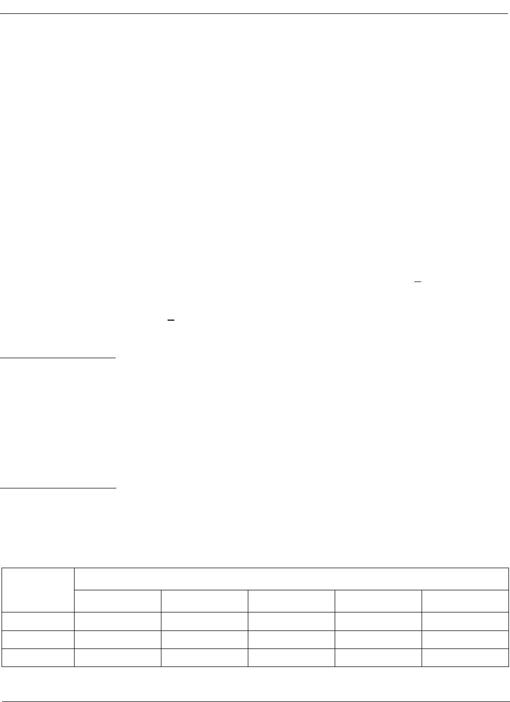
Data Rate Throughput Delay (d)
2.048 Mb/s d=[32 + (32 - IN) + (OUT - 1)]; (expressed in # time-slots)
2.048 Mb/s time-slot: 3.9s
IN: input time-slot (from 1 to 32)
OUT: output time-slot (from 1 to 32)
4.096 Mb/s d=[64 + (64 - IN) + (OUT - 1)]; (expressed in # time-slots)
4.096 Mb/s time-slot: 1.95 s
IN: input time-slot (from 1 to 64)
OUT: output time-slot (from 1 to 64)
8.192 Mb/s d=[128 + (128 - IN) + (OUT - 1)]; (expressed in # time-slots)
8.192 Mb/s time-slot: 0.975 s
IN: input time-slot (from 1 to 128)
OUT: output time-slot (from 1 to 128)

MT89L86APR1

Mfr. #:
Manufacturer:
Microchip / Microsemi
Description:
Digital Bus Switch ICs Pb Free LOW VOLTAGE MULTIRATE DIGITL SW
Lifecycle:
New from this manufacturer.
Delivery:
DHL FedEx Ups TNT EMS
Payment:
T/T Paypal Visa MoneyGram Western Union

Products related to this Datasheet