Figure 4: Functional Block Diagram, PCB 1486 (R/C A1)
U12
DQ0
DQ1
DQ2
DQ3
DQ4
DQ5
DQ6
DQ7
DQ
DQ
DQ
DQ
DQ
DQ
DQ
DQ
ZQ
DM/ NF/ CS# DQS DQS#
TDQS TDQS#
DQ
DQ
DQ
DQ
DQ
DQ
DQ
DQ
ZQ
DQ32
DQ33
DQ34
DQ35
DQ36
DQ37
DQ38
DQ39
DM/ NF/ CS# DQS DQS#
TDQS TDQS#
RS0#
U5
DQ
DQ
DQ
DQ
DQ
DQ
DQ
DQ
ZQ
DQ8
DQ9
DQ10
DQ11
DQ12
DQ13
DQ14
DQ15
DM/ NF/ CS# DQS DQS#
TDQS TDQS#
DQ
DQ
DQ
DQ
DQ
DQ
DQ
DQ
ZQ
DQ40
DQ41
DQ42
DQ43
DQ44
DQ45
DQ46
DQ47
DM/ NF/ CS# DQS DQS#
TDQS TDQS#
U9
U2
DQ
DQ
DQ
DQ
DQ
DQ
DQ
DQ
ZQ
DQ16
DQ17
DQ18
DQ19
DQ20
DQ21
DQ22
DQ23
DM/ NF/ CS# DQS DQS#
TDQS TDQS#
DQ
DQ
DQ
DQ
DQ
DQ
DQ
DQ
ZQ
DQ48
DQ49
DQ50
DQ51
DQ52
DQ53
DQ54
DQ55
DM/ NF/ CS# DQS DQS#
TDQS TDQS#
DQ
DQ
DQ
DQ
DQ
DQ
DQ
DQ
ZQ
DQ24
DQ25
DQ26
DQ27
DQ28
DQ29
DQ30
DQ31
DM/ NF/ CS# DQS DQS#
TDQS TDQS#
DQ
DQ
DQ
DQ
DQ
DQ
DQ
DQ
ZQ
DQ56
DQ57
DQ58
DQ59
DQ60
DQ61
DQ62
DQ63
DM/ NF/ CS# DQS DQS#
TDQS TDQS#
DQ
DQ
DQ
DQ
DQ
DQ
DQ
DQ
ZQ
CB0
CB1
CB2
CB3
CB4
CB5
CB6
CB7
DM/ NF/ CS# DQS DQS#
TDQS TDQS#
U11
U3
U10
U8
U6
V
REFCA
V
SS
DDR3 SDRAM
DDR3 SDRAM
V
DD
Conrol, command and
address termination
V
DDSPD
V
TT
DDR3 SDRAM
DDR3 SDRAM
V
REFDQ
V
SS
V
SS
V
SS
V
SS
V
SS
V
SS
V
SS
V
SS
V
SS
EVENT#
U1
SA0 SA1
SA2
A0
SPD EEPROM/
Temperature
sensor
A1 A2
SDA
SCL
EVT
RS0#, RCKE0, RA[15/14/13:0],
RRAS#, RCAS#, RWE#,
RODT0, RBA[2:0]
Command, control, address, and clock line terminations:
DDR3
SDRAM
V
TT
DDR3
SDRAM
V
DD
SPD EEPROM/
Temperature sensor
R
e
g
i
s
t
e
r
a
n
d
P
L
L
S1#
S0#
BA[2:0]
A[15:0]
RAS#
CAS#
WE#
CKE0
ODT0
Par _In
RESET#
CK0
CK0#
RS0#: DDR3 SDRAM
RBA[2:0]: DDR3 SDRAM
RA[15/14/13:0]: DDR3 SDRAM
RRAS#: DDR3 SDRAM
RCAS#: DDR3 SDRAM
RWE#: DDR3 SDRAM
RCKE0: DDR3 SDRAM
RODT0: DDR3 SDRAM
Err _Out #
U4
CK0[A:B]
CK0#[A:B]
DDR3 SDRAM
DDR3 SDRAM
CKE1
VSS
ODT1
DQS0
DQS0#
DQS9
DQS9#
DQS4
DQS4#
DQS13
DQS13#
DQS1
DQS1#
DQS10
DQS10#
DQS5
DQS5#
DQS14
DQS14#
DQS2
DQS2#
DQS11
DQS11#
DQS6
DQS6#
DQS15
DQS15#
DQS3
DQS3#
DQS12
DQS12#
DQS7
DQS7#
DQS16
DQS16#
DQS8
DQS8#
DQS17
DQS17#
CK0[A:B]
CK0#[A:B]
Note:
1. The ZQ ball on each DDR3 component is connected to an external 240Ω ±1% resistor
that is tied to ground. It is used for the calibration of the component’s ODT and output
driver.
2GB, 4GB (x72, ECC, SR) 240-Pin DDR3L RDIMM
Functional Block Diagrams
PDF: 09005aef83b2f73b
ksf9c256_512x72pz.pdf - Rev. I 7/15 EN
10
Micron Technology, Inc. reserves the right to change products or specifications without notice.
© 2009 Micron Technology, Inc. All rights reserved.
General Description
DDR3 SDRAM modules are high-speed, CMOS dynamic random access memory mod-
ules that use internally configured 8-bank DDR3 SDRAM devices. DDR3 SDRAM mod-
ules use DDR architecture to achieve high-speed operation. DDR3 architecture is essen-
tially an 8n-prefetch architecture with an interface designed to transfer two data words
per clock cycle at the I/O pins. A single read or write access for the DDR3 SDRAM mod-
ule effectively consists of a single 8n-bit-wide, one-clock-cycle data transfer at the inter-
nal DRAM core and eight corresponding n-bit-wide, one-half-clock-cycle data transfers
at the I/O pins.
DDR3 modules use two sets of differential signals: DQS, DQS# to capture data and CK
and CK# to capture commands, addresses, and control signals. Differential clocks and
data strobes ensure exceptional noise immunity for these signals and provide precise
crossing points to capture input signals.
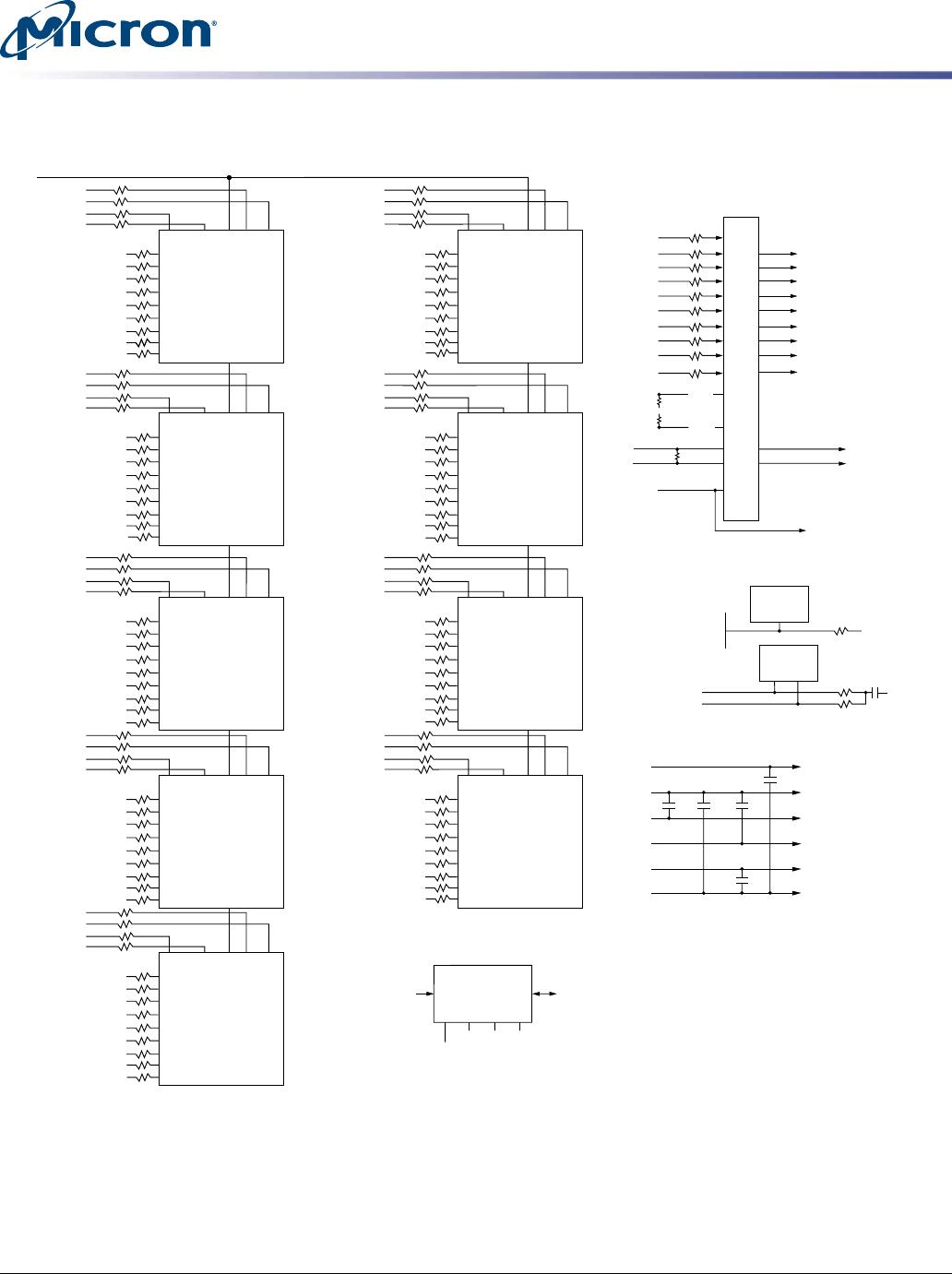
Fly-By Topology
DDR3 modules use faster clock speeds than earlier DDR technologies, making signal
quality more important than ever. For improved signal quality, the clock, control, com-
mand, and address buses have been routed in a fly-by topology, where each clock, con-
trol, command, and address pin on each DRAM is connected to a single trace and ter-
minated (rather than a tree structure, where the termination is off the module near the
connector). Inherent to fly-by topology, the timing skew between the clock and DQS sig-
nals can be easily accounted for by using the write-leveling feature of DDR3.
Registering Clock Driver Operation
Registered DDR3 SDRAM modules use a registering clock driver device consisting of a
register and a phase-lock loop (PLL). The device complies with the JEDEC standard
"Definition of the SSTE32882 Registering Clock Driver with Parity and Quad Chip Se-
lects for DDR3 RDIMM Applications."
The register section of the registering clock driver latches command and address input
signals on the rising clock edge. The PLL section of the registering clock driver receives
and redrives the differential clock signals (CK, CK#) to the DDR3 SDRAM devices. The
register(s) and PLL reduce clock, control, command, and address signals loading by iso-
lating DRAM from the system controller.
Parity Operations
The registering clock driver includes an even parity function for checking parity. The
memory controller accepts a parity bit at the Par_In input and compares it with the data
received on A[15:0], BA[2:0], RAS#, CAS#, and WE#. Valid parity is defined as an even
number of ones (1s) across the address and command inputs (A[15:0], BA[2:0], RAS#,
CAS#, and WE#) combined with Par_In. Parity errors are flagged on Err_Out#.
Address and command parity is checked during all DRAM operations and during con-
trol word WRITE operations to the registering clock driver. For SDRAM operations, the
address is still propagated to the SDRAM even when there is a parity error. When writ-
ing to the internal control words of the registering clock driver, the write will be ignored
if parity is not valid. For this reason, systems must connect the Par_In pins on the
DIMM and provide correct parity when writing to the registering clock driver control
word configuration registers.
2GB, 4GB (x72, ECC, SR) 240-Pin DDR3L RDIMM
General Description
PDF: 09005aef83b2f73b
ksf9c256_512x72pz.pdf - Rev. I 7/15 EN
11
Micron Technology, Inc. reserves the right to change products or specifications without notice.
© 2009 Micron Technology, Inc. All rights reserved.
Temperature Sensor with Serial Presence-Detect EEPROM
Thermal Sensor Operations
The temperature from the integrated thermal sensor is monitored and converts into a
digital word via the I
2
C bus. System designers can use the user-programmable registers
to create a custom temperature-sensing solution based on system requirements. Pro-
gramming and configuration details comply with JEDEC standard No. 21-C page 4.7-1,
"Definition of the TSE2002av, Serial Presence Detect with Temperature Sensor."
Serial Presence-Detect EEPROM Operation
DDR3 SDRAM modules incorporate serial presence-detect. The SPD data is stored in a
256-byte EEPROM. The first 128 bytes are programmed by Micron to comply with JE-
DEC standard JC-45, "Appendix X: Serial Presence Detect (SPD) for DDR3 SDRAM Mod-
ules." These bytes identify module-specific timing parameters, configuration informa-
tion, and physical attributes. The remaining 128 bytes of storage are available for use by
the customer. System READ/WRITE operations between the master (system logic) and
the slave EEPROM device occur via a standard I
2
C bus using the DIMM’s SCL (clock)
SDA (data), and SA (address) pins. Write protect (WP) is connected to V
SS
, permanently
disabling hardware write protection. For further information refer to Micron technical
note TN-04-42, "Memory Module Serial Presence-Detect."
2GB, 4GB (x72, ECC, SR) 240-Pin DDR3L RDIMM
Temperature Sensor with Serial Presence-Detect EEPROM
PDF: 09005aef83b2f73b
ksf9c256_512x72pz.pdf - Rev. I 7/15 EN
12
Micron Technology, Inc. reserves the right to change products or specifications without notice.
© 2009 Micron Technology, Inc. All rights reserved.

MT9KSF51272PZ-1G6E2

Mfr. #:
Manufacturer:
Micron
Description:
MODULE DDR3L SDRAM 4GB 240RDIMM
Lifecycle:
New from this manufacturer.
Delivery:
DHL FedEx Ups TNT EMS
Payment:
T/T Paypal Visa MoneyGram Western Union

Products related to this Datasheet