Electrical Specifications
Stresses greater than those listed may cause permanent damage to the module. This is a
stress rating only, and functional operation of the module at these or any other condi-
tions outside those indicated in each device's data sheet is not implied. Exposure to ab-
solute maximum rating conditions for extended periods may adversely affect reliability.
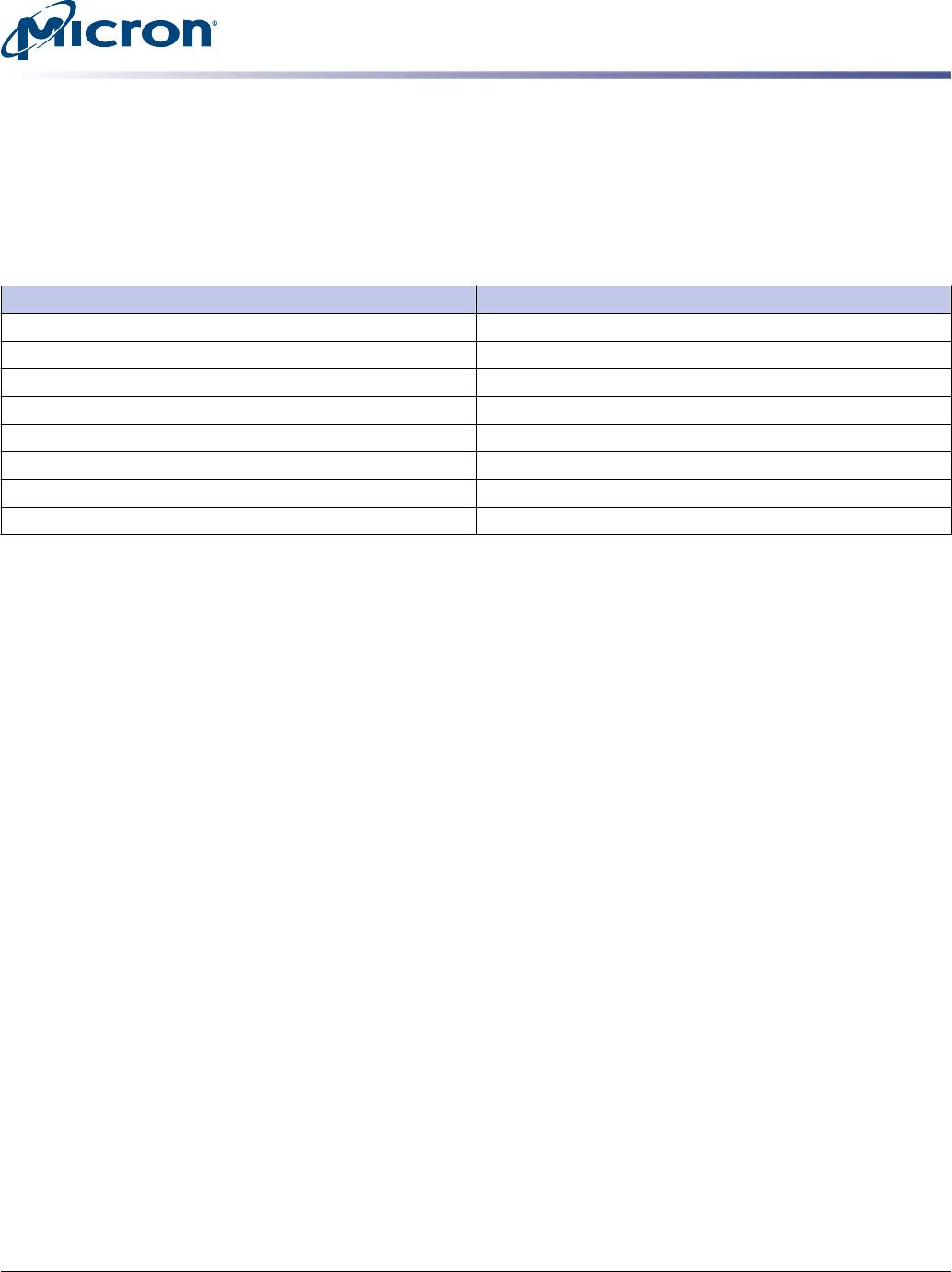
Table 9: Absolute Maximum Ratings
Symbol Parameter Min Max Units
V
DD
V
DD
supply voltage relative to V
SS
–0.4 1.975 V
V
IN
, V
OUT
Voltage on any pin relative to V
SS
–0.4 1.975 V
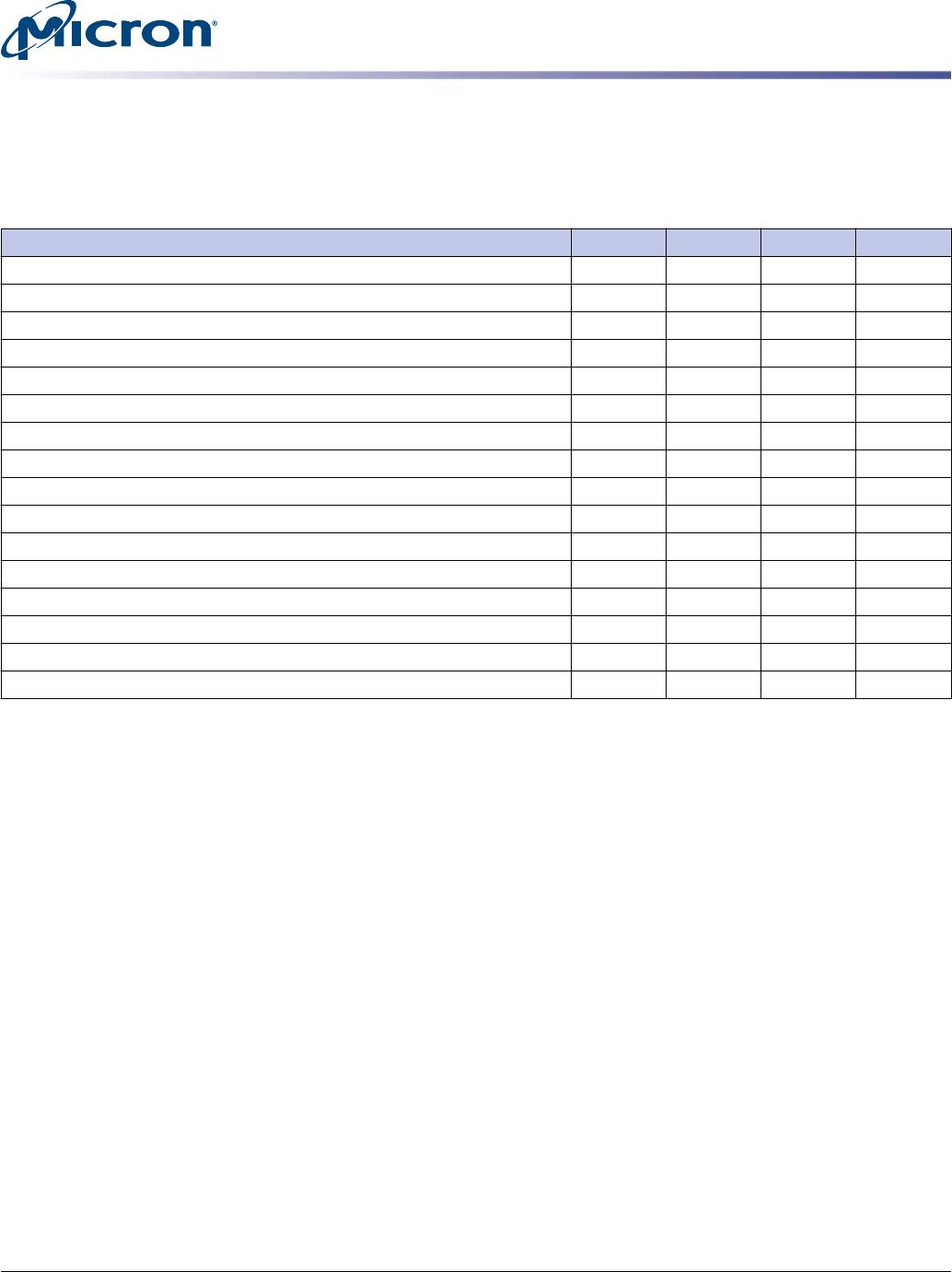
Table 10: Operating Conditions
Symbol Parameter Min Nom Max Units Notes
V
DD
V
DD
supply voltage 1.283 1.35 1.45 V
1.425 1.5 1.575 V 1
V
REFCA(DC)
Input reference voltage command/address bus 0.49 × V
DD
0.5 × V
DD
0.51 × V
DD
V
V
REFDQ(DC)
I/O reference voltage DQ bus 0.49 × V
DD
0.5 × V
DD
0.51 × V
DD
V
I
VTT
Termination reference current from V
TT
–600 600 mA
V
TT
Termination reference voltage (DC) – command/
address bus
0.49 × V
DD
-
20mV
0.5 × V
DD
0.51 × V
DD
+
20mV
V 2
I
I
Input leakage current; Any input
0V V
IN
V
DD
; V
REF
input 0V V
IN
0.95V (All other pins not under
test = 0V)
Address in-
puts, RAS#,
CAS#, WE#,
S#, CKE, ODT,
BA, CK, CK#
µA 6
I
OZ
Output leakage current; 0V V
OUT
V
DD
; DQ and ODT are disabled;
ODT is HIGH
DQ, DQS,
DQS#
–5 0 5 µA
I
VREF
V
REF
supply leakage current; V
REFDQ
= V
DD/2
or
V
REFCA
= V
DD/2
(All other pins not under test = 0V)
–9 0 9 µA
T
A
Module ambient operating tem-
perature
Commercial 0 70 °C 3, 4
T
C
DDR3 SDRAM component case op-
erating temperature
Commercial 0 95 °C 3, 4, 5
Notes:
1. Module is backward-compatible with 1.5V operation. Refer to device specification for
details and operation guidance.
2. V
TT
termination voltage in excess of the stated limit will adversely affect the command
and address signals’ voltage margin and will reduce timing margins.
3. T
A
and T
C
are simultaneous requirements.
4. For further information, refer to technical note TN-00-08: “Thermal Applications,”
available on Micron’s Web site.
5. The refresh rate is required to double when 85°C < T
C
95°C.
6. Inputs are terminated to V
DD
/2. Input current is dependent on terminating resistance se-
lected in register.
2GB, 4GB (x72, ECC, SR) 240-Pin DDR3L RDIMM
Electrical Specifications
PDF: 09005aef83b2f73b
ksf9c256_512x72pz.pdf - Rev. I 7/15 EN
13
Micron Technology, Inc. reserves the right to change products or specifications without notice.
© 2009 Micron Technology, Inc. All rights reserved.
DRAM Operating Conditions
Recommended AC operating conditions are given in the DDR3 component data sheets.
Component specifications are available at micron.com. Module speed grades correlate
with component speed grades, as shown below.
Table 11: Module and Component Speed Grades
DDR3 components may exceed the listed module speed grades; module may not be available in all listed speed grades
Module Speed Grade Component Speed Grade
-2G1 -093
-1G9 -107
-1G6 -125
-1G4 -15E
-1G1 -187E
-1G0 -187
-80C -25E
-80B -25
Design Considerations
Simulations
Micron memory modules are designed to optimize signal integrity through carefully de-
signed terminations, controlled board impedances, routing topologies, trace length
matching, and decoupling. However, good signal integrity starts at the system level.
Micron encourages designers to simulate the signal characteristics of the system's
memory bus to ensure adequate signal integrity of the entire memory system.
Power
Operating voltages are specified at the DRAM, not at the edge connector of the module.
Designers must account for any system voltage drops at anticipated power levels to en-
sure the required supply voltage is maintained.
2GB, 4GB (x72, ECC, SR) 240-Pin DDR3L RDIMM
DRAM Operating Conditions
PDF: 09005aef83b2f73b
ksf9c256_512x72pz.pdf - Rev. I 7/15 EN
14
Micron Technology, Inc. reserves the right to change products or specifications without notice.
© 2009 Micron Technology, Inc. All rights reserved.
I
DD
Specifications
Table 12: DDR3 I
DD
Specifications and Conditions – 2GB (Die Revision K)
Values are for the MT41K256M8 DDR3L SDRAM only and are computed from values specified in the 2Gb (256 Meg x 8)
1.35V component data sheet
Parameter Symbol 1600 1333 Units
Operating current 0: One bank ACTIVATE-to-PRECHARGE I
DD0
351 342 mA
Operating current 1: One bank ACTIVATE-to-READ-to-PRECHARGE I
DD1
468 450 mA
Precharge power-down current: Slow exit I
DD2P0
108 108 mA
Precharge power-down current: Fast exit I
DD2P1
126 126 mA
Precharge quiet standby current I
DD2Q
180 180 mA
Precharge standby current I
DD2N
189 189 mA
Precharge standby ODT current I
DD2NT
279 261 mA
Active power-down current I
DD3P
189 189 mA
Active standby current I
DD3N
288 270 mA
Burst read operating current I
DD4R
846 738 mA
Burst write operating current I
DD4W
873 765 mA
Refresh current I
DD5B
1620 1611 mA
Self refresh temperature current: MAX T
C
= 85°C I
DD6
108 108 mA
Self refresh temperature current (SRT-enabled): MAX T
C
= 95°C I
DD6ET
135 135 mA
All banks interleaved read current I
DD7
1404 1350 mA
Reset current I
DD8
126 126 mA
2GB, 4GB (x72, ECC, SR) 240-Pin DDR3L RDIMM
I
DD
Specifications
PDF: 09005aef83b2f73b
ksf9c256_512x72pz.pdf - Rev. I 7/15 EN
15
Micron Technology, Inc. reserves the right to change products or specifications without notice.
© 2009 Micron Technology, Inc. All rights reserved.

MT9KSF51272PZ-1G6E2

Mfr. #:
Manufacturer:
Micron
Description:
MODULE DDR3L SDRAM 4GB 240RDIMM
Lifecycle:
New from this manufacturer.
Delivery:
DHL FedEx Ups TNT EMS
Payment:
T/T Paypal Visa MoneyGram Western Union

Products related to this Datasheet