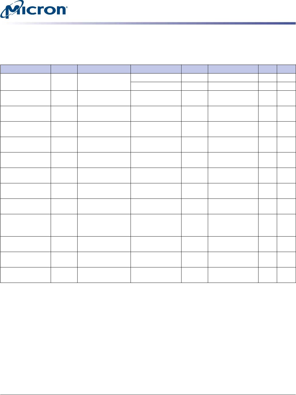
Table 13: DDR3 I
DD
Specifications and Conditions – 4GB (Die Revision E)
Values are for the MT41K512M8 DDR3L SDRAM only and are computed from values specified in the 4Gb (512 Meg x 8)
1.35V component data sheet
Parameter Symbol 1600 1333 Units
Operating current 0: One bank ACTIVATE-to-PRECHARGE I
DD0
495 423 mA
Operating current 1: One bank ACTIVATE-to-READ-to-PRECHARGE I
DD1
594 558 mA
Precharge power-down current: Slow exit I
DD2P0
162 162 mA
Precharge power-down current: Fast exit I
DD2P1
288 252 mA
Precharge quiet standby current I
DD2Q
288 252 mA
Precharge standby current I
DD2N
288 261 mA
Precharge standby ODT current I
DD2NT
351 315 mA
Active power-down current I
DD3P
342 315 mA
Active standby current I
DD3N
342 315 mA
Burst read operating current I
DD4R
1413 1260 mA
Burst write operating current I
DD4W
1125 990 mA
Refresh current I
DD5B
2115 2052 mA
Self refresh temperature current: MAX T
C
= 85°C I
DD6
180 180 mA
Self refresh temperature current (SRT-enabled): MAX T
C
= 95°C I
DD6ET
225 225 mA
All banks interleaved read current I
DD7
1980 1710 mA
Reset current I
DD8
180 180 mA
2GB, 4GB (x72, ECC, SR) 240-Pin DDR3L RDIMM
I
DD
Specifications
PDF: 09005aef83b2f73b
ksf9c256_512x72pz.pdf - Rev. I 7/15 EN
16
Micron Technology, Inc. reserves the right to change products or specifications without notice.
© 2009 Micron Technology, Inc. All rights reserved.
Table 14: DDR3 I
DD
Specifications and Conditions – 4GB (Die Revision P)
Values are for the MT41K512M8 DDR3L SDRAM only and are computed from values specified in the 4Gb (512 Meg x 8)
1.35V component data sheet
Parameter Symbol 1600 Units
Operating current 0: One bank ACTIVATE-to-PRECHARGE I
DD0
252 mA
Operating current 1: One bank ACTIVATE-to-READ-to-PRECHARGE I
DD1
387 mA
Precharge power-down current: Slow exit I
DD2P0
90 mA
Precharge power-down current: Fast exit I
DD2P1
99 mA
Precharge quiet standby current I
DD2Q
135 mA
Precharge standby current I
DD2N
144 mA
Precharge standby ODT current I
DD2NT
180 mA
Active power-down current I
DD3P
135 mA
Active standby current I
DD3N
180 mA
Burst read operating current I
DD4R
810 mA
Burst write operating current I
DD4W
909 mA
Refresh current I
DD5B
1368 mA
Self refresh temperature current: MAX T
C
= 85°C I
DD6
135 mA
Self refresh temperature current (SRT-enabled): MAX T
C
= 95°C I
DD6ET
207 mA
All banks interleaved read current I
DD7
1170 mA
Reset current I
DD8
117 mA
2GB, 4GB (x72, ECC, SR) 240-Pin DDR3L RDIMM
I
DD
Specifications
PDF: 09005aef83b2f73b
ksf9c256_512x72pz.pdf - Rev. I 7/15 EN
17
Micron Technology, Inc. reserves the right to change products or specifications without notice.
© 2009 Micron Technology, Inc. All rights reserved.
Registering Clock Driver Specifications
Table 15: Registering Clock Driver Electrical Characteristics
SSTE32882 devices or equivalent; Note 1 applies to entire table
Parameter Symbol Pins Min Nom Max Units Notes
DC supply voltage V
DD
1.283 1.35 1.45 V
1.425 1.5 1.575 V 2
DC reference volt-
age
V
REF
0.49 × V
DD
- 20mV 0.5 × V
DD
0.51 × V
DD
+ 20mV V
DC termination
voltage
V
TT
0.49 × V
DD
- 20mV 0.5 × V
DD
0.51 × V
DD
+ 20mV V
AC high-level input
voltage
V
IH(AC)
Control, command,
address
V
REF
+ 175mV V
DD
+ 400mV V
AC low-level input
voltage
V
IL(AC)
Control, command,
address
–0.4 V
REF
- 175mV V
DC high-level input
voltage
V
IH(DC)
Control, command,
address
V
REF
+ 100mV V
DD
+ 0.4 V
DC low-level input
voltage
V
IL(DC)
Control, command,
address
–0.4 V
REF
- 100mV V
High-level input
voltage
V
IH(CMOS)
RESET#, MIRROR 0.65 × V
DD
V
DD
V
Low-level input
voltage
V
IL(CMOS)
RESET#, MIRROR 0 0.35 × V
DD
V
Differential input
crosspoint voltage
range
V
IX(AC)
CK, CK#, FBIN, FBIN# 0.5 × V
DD
- 175mV 0.5 × V
DD
0.5 × V
DD
+ 175mV V
Differential input
voltage
V
ID(AC)
CK, CK# 350 V
DD
+ TBD mV
High-level output
current
I
OH
Err_Out# TBD mA
Low-level output
current
I
OL
Err_Out# TBD TBD mA
Notes:
1. Timing and switching specifications for the register listed are critical for proper opera-
tion of the DDR3 SDRAM RDIMMs. These are meant to be a subset of the parameters for
the specific device used on the module.
2. The register is backward-compatible with 1.5V operation. Refer to device specification
for details and operation guidance.
2GB, 4GB (x72, ECC, SR) 240-Pin DDR3L RDIMM
Registering Clock Driver Specifications
PDF: 09005aef83b2f73b
ksf9c256_512x72pz.pdf - Rev. I 7/15 EN
18
Micron Technology, Inc. reserves the right to change products or specifications without notice.
© 2009 Micron Technology, Inc. All rights reserved.

MT9KSF51272PZ-1G6E2

Mfr. #:
Manufacturer:
Micron
Description:
MODULE DDR3L SDRAM 4GB 240RDIMM
Lifecycle:
New from this manufacturer.
Delivery:
DHL FedEx Ups TNT EMS
Payment:
T/T Paypal Visa MoneyGram Western Union

Products related to this Datasheet