2002-2012 Microchip Technology Inc. DS21457D-page 1
TC7116/A/TC7117/A
Features:
Low Temperature Drift Internal Reference:
- TC7116/TC7117 80 ppm/°C, Typ.
- TC7116A/TC7117A 20 ppm/°C, Typ.
Display Hold Function
Directly Drives LCD or LED Display
Zero Reading with Zero Input
Low Noise for Stable Display:
- 2V or 200mV Full Scale Range (FSR)
Auto-Zero Cycle Eliminates Need for Zero
Adjustment Potentiometer
True Polarity Indication for Precision Null
Applications
Convenient 9V Battery Operation:
(TC7116/TC7116A)
High-Impedance CMOS Differential Inputs: 10
12
Low-Power Operation: 10mW
Applications:
Thermometry
Bridge Readouts: Strain Gauges, Load Cells,
Null Detectors
Digital Meters: Voltage/Current/Ohms/Power, pH
Digital Scales, Process Monitors
Portable Instrumentation
Device Selection Table
General Description:
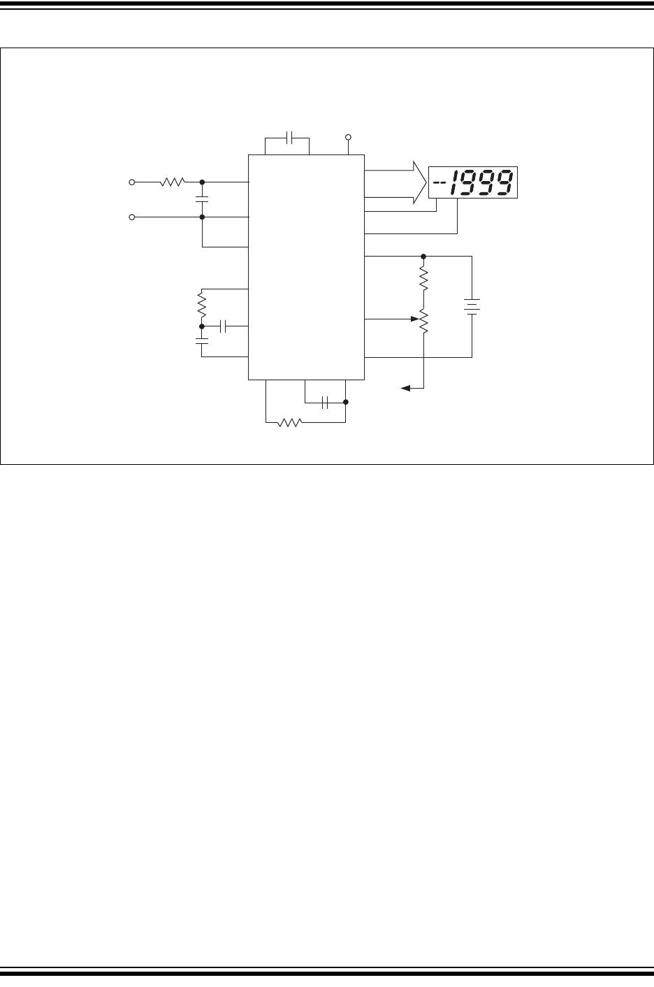
The TC7116A/TC7117A are 3-1/2 digit CMOS Analog-
to-Digital Converters (ADCs) containing all the active
components necessary to construct a 0.05% resolution
measurement system. Seven-segment decoders,
polarity and digit drivers, voltage reference, and clock
circuit are integrated on-chip. The TC7116A drives
Liquid Crystal Displays (LCDs) and includes a back-
plane driver. The TC7117A drives common anode Light
Emitting Diode (LED) displays directly with an 8mA
drive current per segment.
These devices incorporate a display hold (HLDR)
function. The displayed reading remains indefinitely, as
long as HLDR is held high. Conversions continue, but
output data display latches are not updated. The refer-
ence low input (V
REF
-) is not available, as it is with the
TC7106/7107. V
REF
-
is tied internally to analog
common in the TC7116A/7117A devices.
The TC7116A/7117A reduces linearity error to less
than 1 count. Rollover error (the difference in readings
for equal magnitude but opposite polarity input signals)
is below ±1 count. High-impedance differential inputs
offer 1pA leakage current and a 10
12
input imped-
ance. The 15V
P-P
noise performance enables a “rock
solid” reading. The auto-zero cycle ensures a zero
display reading with a 0V input.
The TC7116A and TC7117A feature a precision, low
drift internal reference, and are functionally identical to
the TC7116/TC7117. A low drift external reference is
not normally required with the TC7116A/TC7117A.
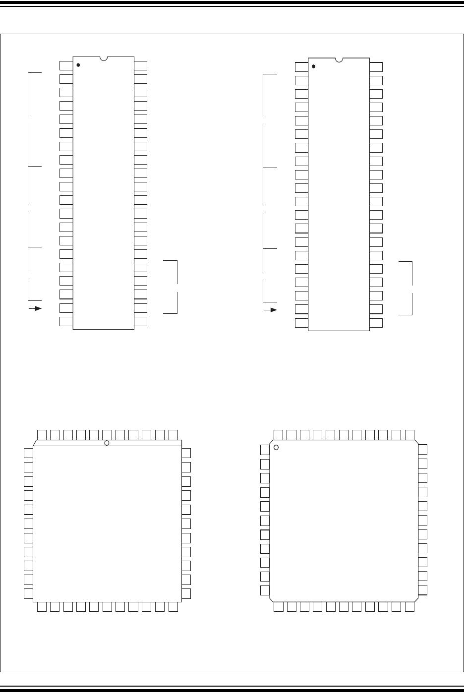
Package Code Package Temperature Range
CPL 40-Pin PDIP 0C to +70C
IJL 40-Pin CERDIP -25C to +85C
CKW 44-Pin PQFP 0C to +70C
CLW 44-Pin PLCC 0C to +70C
3-1/2 Digit Analog-to-Digital Converters with Hold
TC7116/A/TC7117/A
DS21457D-page 2 2002-2012 Microchip Technology Inc.
Package Type
BP/
GND
33
34
35
36
37
38
39
13
10
9
8
7
COMMON
V+
18 19 20 21 23 24
AB
4
POL
NC
V
IN
+
NC
V
IN
-
B2
6543 1442
A
1
OSC1
22
43
OSC2
42
OSC3
41
TEST
40
V
REF
+
25 26 27 28
F
3
E
3
G
3
A
3
C
3
G
2
3214
C
AZ
3115
V
BUFF
3016
V
INT
E
2
2917
D
3
NC
11
12
NC
C
2
D
2
F
2
A
2
B
3
TC7116CLW
TC7116ACLW
TC7117CLW
TC7117ACLW
TC7116CPL
TC7116ACPL
TC7117CPL
TC7117ACPL
V-
C
REF
+
C
REF
-
B
1
C
1
D
1
F
1
G
1
E
1
BP/
GND
27
28
29
30
31
32
33
7
4
3
2
1
NC
TC7116CKW
TC7116ACKW
TC7117CKW
TC7117ACKW
12 13 14 15 17 18
G
3
44 43 42 41 39 3840
V
REF
+
COMMON
16
37
C
AZ
36
V
BUFF
35
V
INT
34
V-
19 20 21 22
D
3
26
8
25
9
24
10
23
11
V
IN
+
5
6
C
3
OSC3
TEST
NC
NC
HLDR
D
2
C
2
B
2
A
2
F
2
E
2
NC
OSC2
OSC1
V+
C
REF
+
C
REF
-
V
IN
-
A
3
G
3
POL
AB
4
E
3
F
3
B
3
D
1
C
1
B
1
A
1
F
1
G
1
E
1
40-Pin PDIP 40-Pin CERDIP
44-Pin PLCC 44-Pin PQFP
1
2
3
4
OSC1
5
6
7
8
9
10
11
12
TEST
V
REF
+
COMMON
C
AZ
HLDR
D
2
13
14
15
16
17
18
19
20
40
39
38
37
36
35
34
33
32
31
30
29
28
27
26
25
24
23
22
21
C
2
B
2
A
2
F
2
E
2
D
3
B
3
F
3
E
3
AB
4
(Minus Sign)
(Minus Sign)
10's
100's
1000's
(TC7116/7117)
(TC7116A/TC7117A)
(TC7116/7117)
(TC7116A/TC7117A)
100's
OSC2
OSC3
V+
C
REF
+
C
REF
-
V
IN
+
V
IN
-
V
BUFF
V
INT
V-
G
2
C
3
A
3
G
3
BP/GND
POL
D
1
C
1
B
1
A
1
F
1
G
1
E
1
1's
HLDR
TC7116IJL
TC7116AIJL
TC7117IJL
TC7117AIJL
1
2
3
4
OSC1
5
6
7
8
9
10
11
12
TEST
V
REF
+
COMMON
C
AZ
HLDR
D
2
13
14
15
16
17
18
19
20
40
39
38
37
36
35
34
33
32
31
30
29
28
27
26
25
24
23
22
21
C
2
B
2
A
2
F
2
E
2
D
3
B
3
F
3
E
3
AB
4
10's
100's
1000's
100's
OSC2
OSC3
V+
C
REF
+
C
REF
-
V
IN
+
V
IN
-
V
BUFF
V
INT
V-
G
2
C
3
A
3
G
3
BP/GND
POL
D
1
C
1
B
1
A
1
F
1
G
1
E
1
1's
Note 1: NC = No internal connection.
2: Pins 9, 25, 40 and 56 are connected to the die substrate. The potential at these pins is approximately V+. No
external connections should be made.
2002-2012 Microchip Technology Inc. DS21457D-page 3
TC7116/A/TC7117/A
Typical Application
V
REF
+
TC7116/A
9V
V
REF
33
34
24kΩ
1kΩ
31
29
36
39 38
40
0.47μF
0.1μF
V-
OSC1OSC3
OSC2
To Analog
Common (Pin 32)
3 Conversions Per Second
C
OSC
100kΩ
47kΩ
0.22μF
0.01μF
Analog
Input
+
C
REF
-C
REF
+
V
IN
+
V
IN
-
ANALOG
COMMON
V
INT
V
BUFF
C
AZ
20
21
35
Segment
Drive
2–19
22–25
POL
BP/GND
V+
Minus Sign
Backplane Drive
28
R
OSC
100pF
LCD Display (TC7116/7116A)
or Common Anode LED Display
(TC7117/7117A)
1MΩ
27
30
32
HLDR
Display
Hold
100mV
1
26
TC7117/A
+

TC7117ACLW

Mfr. #:
Manufacturer:
Microchip Technology
Description:
LED Display Drivers w/Hold
Lifecycle:
New from this manufacturer.
Delivery:
DHL FedEx Ups TNT EMS
Payment:
T/T Paypal Visa MoneyGram Western Union