TC7116/A/TC7117/A
DS21457D-page 10 2002-2012 Microchip Technology Inc.
FIGURE 3-4: Exclusive “OR” Gate for
Decimal Point Drive
3.2 Digital Section
Figure 3-5 and Figure show the digital section for
TC7116/TC7116A and TC7117/TC7117A, respectively.
For the TC7116/TC7116A (Figure 3-5), an internal dig-
ital ground is generated from a 6V Zener diode and a
large P-channel source follower. This supply is made
stiff to absorb the relative large capacitive currents
when the backplane (BP) voltage is switched. The BP
frequency is the clock frequency 4800. For 3 readings
per second, this is a 60Hz square wave with a nominal
amplitude of 5V. The segments are driven at the same
frequency and amplitude, and are in phase with BP
when OFF, but out of phase when ON. In all cases,
negligible DC voltage exists across the segments.
Figure is the digital section of the TC7117/TC7117A. It
is identical to the TC7116/TC7116A, except that the
regulated supply and BP drive have been eliminated,
and the segment drive is typically 8mA. The 1000’s out-
put (Pin 19) sinks current from two LED segments, and
has a 16mA drive capability. The TC7117/TC7117A are
designed to drive common anode LED displays.
In both devices, the polarity indication is ON for analog
inputs. If V
IN
-
and V
IN
+ are reversed, this indication can
be reversed also, if desired.
FIGURE 3-5: TC7116/TC7116A Digital Section
TC7116
TC7116A
Decimal
Point
Select
V+
V+
TEST
GND
4030
To LCD
Decimal
Point
BP
TC7116
TC7116A
LCD Phase Driver
Thousands
Hundreds
Tens Units
4
Backplane
21
39
37
OSC2
Internal Digital Ground
V+
V-
TES
T
6.2V
500Ω
26
35
To Switch Drivers
From Comparator Output
Clock
V
TH
= 1V
7-Segment
Decode
7-Segment
Decode
7-Segment
Decode
200
40 38
Typical Segment Output
Internal Digital Ground
Segment
Output
V+
0.5mA
2mA
Latch
OSC3OSC1
÷
÷
HLDR
~70kΩ
Logic Control
1
2002-2012 Microchip Technology Inc. DS21457D-page 11
TC7116/A/TC7117/A
3.2.1 SYSTEM TIMING
The clocking method used for the TC7116/TC7116A
and TC7117/TC7117A is shown in Figure . Three
clocking methods may be used:
1. An external oscillator connected to Pin 40.
2. A crystal between Pins 39 and 40.
3. An RC network using all three pins.
The oscillator frequency is 4 before it clocks the
decade counters. It is then further divided to form the
three convert cycle phases: Signal Integrate (1000
counts), Reference De-integrate (0 to 2000 counts),
and Auto-Zero (1000 to 3000 counts). For signals less
than full scale, auto-zero gets the unused portion of ref-
erence de-integrate. This makes a complete measure
cycle of 4000 (16,000 clock pulses), independent of
input voltage. For 3 readings per second, an oscillator
frequency of 48kHz would be used.
To achieve maximum rejection of 60Hz pickup, the sig-
nal integrate cycle should be a multiple of 60Hz. Oscil-
lator frequencies of 240kHz, 120kHz, 80kHz, 60kHz,
48kHz, 40kHz, etc. should be selected. For 50Hz rejec-
tion, oscillator frequencies of 200kHz, 100kHz,
66-2/3kHz, 50kHz, 40kHz, etc. would be suitable. Note
that 40kHz (2.5 readings per second) will reject both
50Hz and 60Hz.
3.2.2 HOLD READING INPUT
When HLDR is at a logic HIGH, the latch will not be
updated. Analog-to-Digital conversions will continue,
but will not be updated until HLDR is returned to LOW.
To continuously update the display, connect to TEST
(TC7116/TC7116A) or GROUND (TC7117/TC7117A),
or disconnect. This input is CMOS compatible with
70k typical resistance to TEST (TC7116/TC7116A) or
GROUND (TC7117/TC7117A).
FIGURE 3-6: TC7117/TC7117A Digital Section
TC7117
TC7117A
4
39
OSC2
V+
Digital
GND
TEST
35
Clock
40 38
OSC3OSC1
÷
HLDR
Control Logic
Typical Segment Output
Digital Ground
To
Segment
V+
0.5mA
8mA
37
21
500Ω
V+
1
Latch
~70kΩ
To Switch Drivers
From Comparator Output
Internal Digital Ground
Thousands
Hundreds Tens
Units
7-Segment
Decode
7-Segment
Decode
7-Segment
Decode
TC7116/A/TC7117/A
DS21457D-page 12 2002-2012 Microchip Technology Inc.
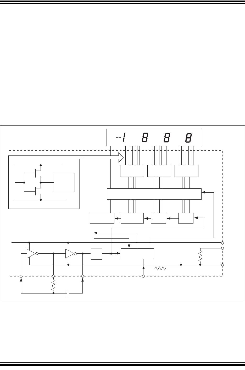
4.0 COMPONENT VALUE
SELECTION
4.1 Auto-Zero Capacitor
The size of the auto-zero capacitor has some influence
on system noise. For 200mV full scale, where noise is
very important, a 0.47F capacitor is recommended.
On the 2V scale, a 0.047F capacitor increases the
speed of recovery from overload and is adequate for
noise on this scale.
4.2 Reference Capacitor
A 0.1F capacitor is acceptable in most applications.
However, where a large Common mode voltage exists
(i.e., the V
IN
- pin is not at analog common), and a
200mV scale is used, a larger value is required to pre-
vent rollover error. Generally, 1F will hold the rollover
error to 0.5 count in this instance.
4.3 Integrating Capacitor
The integrating capacitor should be selected to give the
maximum voltage swing that ensures tolerance buildup
will not saturate the integrator swing (approximately
0.3V from either supply). In the TC7116/TC7116A or
the TC7117/TC7117A, when the analog common is
used as a reference, a nominal ±2V full scale integrator
swing is acceptable. For the TC7117/TC7117A, with
±5V supplies and analog common tied to supply
ground, a ±3.5V to ±4V swing is nominal. For 3 read-
ings per second (48kHz clock), nominal values for C
INT
are 0.221F and 0.10F, respectively. If different oscil-
lator frequencies are used, these values should be
changed in inverse proportion to maintain the output
swing. The integrating capacitor must have low dielec-
tric absorption to prevent rollover errors. Polypropylene
capacitors are recommended for this application.
4.4 Integrating Resistor
Both the buffer amplifier and the integrator have a class
A output stage with 100A of quiescent current. They
can supply 20A of drive current with negligible non-
linearity. The integrating resistor should be large
enough to remain in this very linear region over the
input voltage range, but small enough that undue leak-
age requirements are not placed on the PC board. For
2V full scale, 470k is near optimum and, similarly,
47k for 200mV full scale.
4.5 Oscillator Components
For all frequency ranges, a 100k resistor is recom-
mended; the capacitor is selected from the equation:
EQUATION 4-1:
For a 48kHz clock (3 readings per second), C = 100pF.
4.6 Reference Voltage
To generate full scale output (2000 counts), the analog
input requirement is V
IN
= 2V
REF
. Thus, for the 200mV
and 2V scale, V
REF
should equal 100mV and 1V,
respectively. In many applications, where the ADC is
connected to a transducer, a scale factor exists
between the input voltage and the digital reading. For
instance, in a measuring system, the designer might like
to have a full scale reading when the voltage from the
transducer is 700mV. Instead of dividing the input down
to 200mV, the designer should use the input voltage
directly and select V
REF
= 350mV. Suitable values for
integrating resistor and capacitor would be 120kW and
0.22F. This makes the system slightly quieter and also
avoids a divider network on the input. The TC7117/
TC7117A, with ±5V supplies, can accept input signals
up to ±4V. Another advantage of this system is when a
digital reading of zero is desired for V
IN
0. Tempera-
ture and weighing systems with a variable tare are
examples. This offset reading can be conveniently gen-
erated by connecting the voltage transducer between
V
IN
+ and analog common, and the variable (or fixed)
offset voltage between analog common and V
IN
-.
f
0.45
RC
-------=

TC7117ACLW

Mfr. #:
Manufacturer:
Microchip Technology
Description:
LED Display Drivers w/Hold
Lifecycle:
New from this manufacturer.
Delivery:
DHL FedEx Ups TNT EMS
Payment:
T/T Paypal Visa MoneyGram Western Union