TC7116/A/TC7117/A
DS21457D-page 4 2002-2012 Microchip Technology Inc.
1.0 ELECTRICAL
CHARACTERISTICS
Absolute Maximum Ratings*
Supply Voltage:
TC7116/TC7116A (V+ to V-) ...........................15V
TC7117/TC7117A (V+
to GND).......................+6V
V- to GND.........................................................-9V
Analog Input Voltage (Either Input) (Note 1)... V+ to V-
Reference Input Voltage (Either Input)............ V+ to V-
Clock Input:
TC7116/TC7116A............................... TEST to V+
TC7117/TC7117A.................................GND to V+
Package Power Dissipation; T
A
70°C (Note 2)
40-Pin CDIP................................................2.29W
40-Pin PDIP ................................................1.23W
44-Pin PLCC...............................................1.23W
44-Pin PQFP...............................................1.00W
Operating Temperature:
C (Commercial) Device................... 0°C to +70°C
I (Commercial) Device.................... 0°C to +70°C
Storage Temperature..........................-65°C to +150°C
*Stresses above those listed under “Absolute
Maximum Ratings” may cause permanent damage to
the device. These are stress ratings only and functional
operation of the device at these or any other conditions
above those indicated in the operation sections of the
specifications is not implied. Exposure to Absolute
Maximum Rating conditions for extended periods may
affect device reliability.
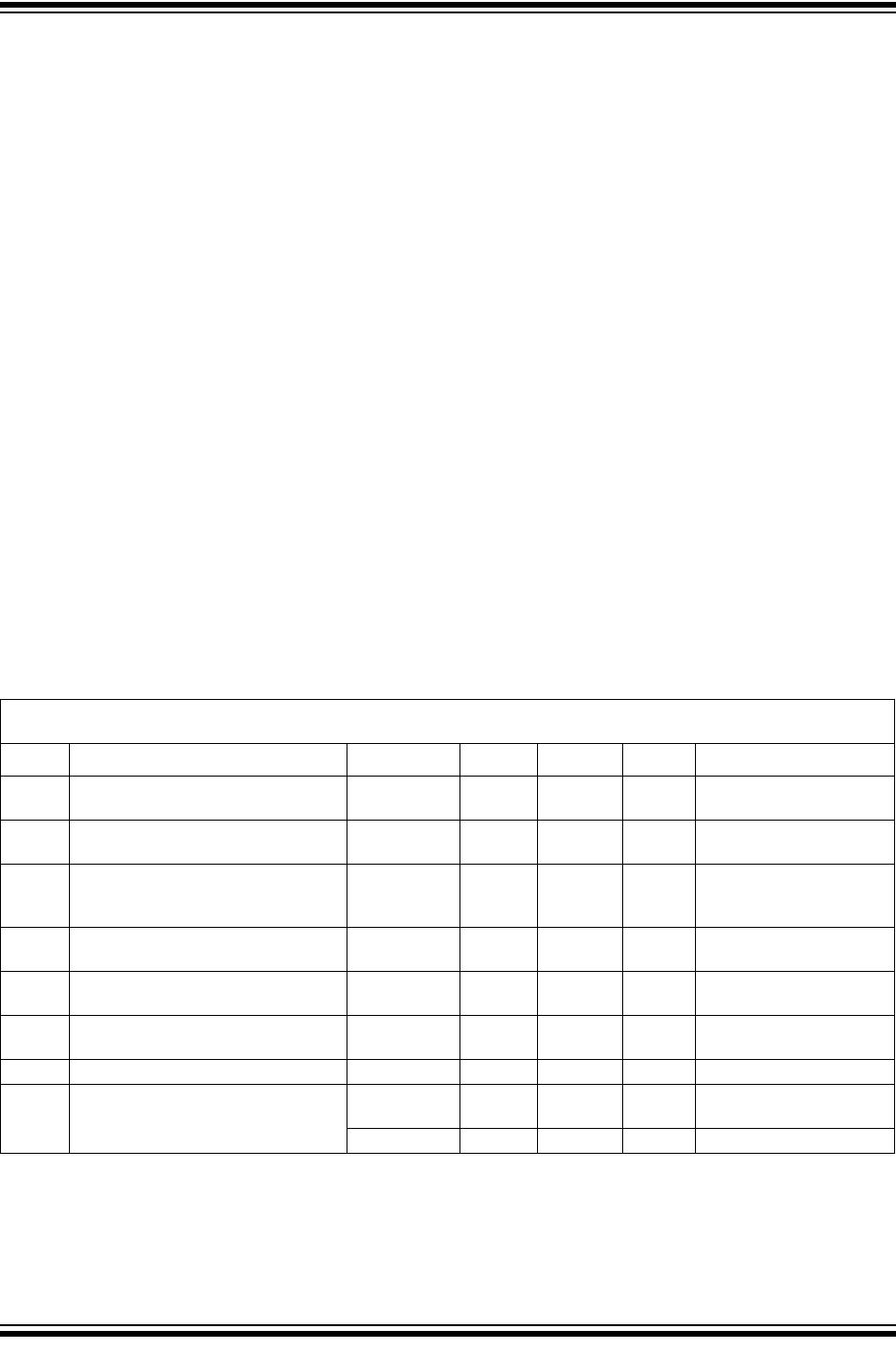
TABLE 1-1: TC7116/A AND TC7117/A ELECTRICAL SPECIFICATIONS
Electrical Characteristics: Unless otherwise noted, specifications apply to both the TC7116/A and TC7117/A at T
A
= 25°C,
f
CLOCK
= 48kHz. Parts are tested in the circuit of the Typical Operating Circuit.
Symbol Parameter Min Typ Max Unit Test Conditions
Z
IR
Zero Input Reading — ±0 — Digital
Reading
V
IN
= 0V
Full Scale = 200mV
Ratiometric Reading 999 999/1000 1000 Digital
Reading
V
IN
= V
REF
V
REF
= 100mV
R/O Rollover Error (Difference in Reading
for Equal Positive and Negative
Readings Near Full Scale)
-1 ±0.2 +1 Counts V
IN
- = + V
IN
+ 200mV
or 2V
Linearity (Maximum Deviation from
Best Straight Line Fit)
-1 ±0.2 +1 Counts Full Scale = 200mV or 2V
CMRR Common Mode Rejection Ratio
(Note 3)
—50—V/V V
CM
= ±1V, V
IN
= 0V
Full Scale = 200mV
e
N
Noise (Peak to Peak 95% of Time) — 15 — VV
IN
= 0V
Full Scale = 200mV
I
L
Leakage Current at Input — 1 10 pA V
IN
= 0V
Zero Reading Drift — 0.2 1 V/°C V
IN
= 0V
“C” Device = 0°C to +70°C
—1.02V/°C “I” Device = -25°C to +85°C
Note 1: Input voltages may exceed the supply voltages provided the input current is limited to ±100A.
2: Dissipation rating assumes device is mounted with all leads soldered to printed circuit board.
3: Refer to “Differential Input” discussion.
4: Backplane drive is in phase with segment drive for “OFF” segment, 180° out of phase for “ON” segment. Frequency is
20 times conversion rate. Average DC component is less than 50mV.
5: The TC7116/TC7116A logic inputs have an internal pull-down resistor connected from HLDR, Pin 1 to TEST, Pin 37. The
TC7117/TC7117A logic inputs have an internal pull-down resistor connected from HLDR, Pin 1 to GND, Pin 21.