2002-2012 Microchip Technology Inc. DS21457D-page 7
TC7116/A/TC7117/A
34 42 C
REF
+A 0.1F capacitor is used in most applications. If a large Common mode voltage
exists (for example, the V
IN
- pin is not at analog common), and a 200mV scale is
used, a 1F capacitor is recommended and will hold the rollover error to
0.5 count.
35 43 V+ Positive Power Supply Voltage.
36 44 V
REF
+ The analog input required to generate a full scale output (1999 counts). Place
100mV between Pins 32 and 36 for 199.9mV full scale. Place 1V between
Pins 35 and 36 for 2V full scale. See Section 4.6 “Reference Voltage”, Refer-
ence Voltage.
37 3 TEST Lamp test. When pulled HIGH (to V+), all segments will be turned on and the dis-
play should read -1888. It may also be used as a negative supply for externally
generated decimal points. See Section 3.1.7 “Test”, TEST for additional infor-
mation.
38 4 OSC3 See Pin 40.
39 6 OSC2 See Pin 40.
40 7 OSC1 Pins 40, 39, 38 make up the oscillator section. For a 48kHz clock (3 readings per
section), connect Pin 40 to the junction of a 100k resistor and a 100pF capaci-
tor. The 100k resistor is tied to Pin 39 and the 100pF capacitor is tied to Pin 38.
TABLE 2-1: PIN FUNCTION TABLE (CONTINUED)
Pin Number
(40-Pin PDIP)
(40-Pin CERDIP)
Pin Number
(44-Pin PQFP)
Symbol Description
TC7116/A/TC7117/A
DS21457D-page 8 2002-2012 Microchip Technology Inc.
3.0 DETAILED DESCRIPTION
(All Pin Designations Refer to 40-Pin PDIP.)
3.1 Analog Section
Figure 3-1 shows the block diagram of the analog sec-
tion for the TC7116/TC7116A and TC7117/TC7117A.
Each measurement cycle is divided into three phases:
(1) Auto-Zero (AZ), (2) Signal Integrate (INT), and
(3) Reference Integrate (REF), or De-integrate (DE).
3.1.1 AUTO-ZERO PHASE
High and low inputs are disconnected from the pins and
internally shorted to analog common. The reference
capacitor is charged to the reference voltage. A feed-
back loop is closed around the system to charge the
auto-zero capacitor (C
AZ
) to compensate for offset volt-
ages in the buffer amplifier, integrator, and comparator.
Since the comparator is included in the loop, AZ
accuracy is limited only by system noise. The offset
referred to the input is less than 10V.
3.1.2 SIGNAL INTEGRATE PHASE
The auto-zero loop is opened, the internal short is
removed, and the internal high and low inputs are
connected to the external pins. The converter then inte-
grates the differential voltages between V
IN
+ and V
IN
-
for a fixed time. This differential voltage can be within a
wide Common mode range: 1V of either supply. How-
ever, if the input signal has no return with respect to the
converter power supply, V
IN
- can be tied to analog
common to establish the correct Common mode
voltage. At the end of this phase, the polarity of the
integrated signal is determined.
FIGURE 3-1: Analog Section of TC7116/TC7116A and TC7117/TC7117A
3.1.3 REFERENCE INTEGRATE PHASE
The final phase is reference integrate, or de-integrate.
Input low is internally connected to analog common
and input high is connected across the previously
charged reference capacitor. Circuitry within the chip
ensures that the capacitor will be connected with the
correct polarity to cause the integrator output to return
to zero. The time required for the output to return to
zero is proportional to the input signal. The digital
reading displayed is:
EQUATION 3-1:
3.1.4 REFERENCE
The positive reference voltage (V
REF
+) is referred to
analog common.
TC7116
TC7116A
TC7117
TC7117A
C
REF
C
REF
+
C
REF
-
R
INT
V+
C
AZ
Auto-Zero
V
INT
28 35 29 27333634
10μA
31
AZ
AZ
INT
AZ & DE (±)
32
30
INT
26
Integrator
V+ -3V
Comparator
To
Digital
Section
DE (+)
DE
(–)
DE
(+)
DE (–)
V+
AZ
Analog
Common
V
IN
+
V
IN
-
V
BUFF
C
INT
V
REF
+
Low
Temp.
Drift
Zener
V
REF
V-
+
+
+
+
1000 =
V
IN
V
REF
2002-2012 Microchip Technology Inc. DS21457D-page 9
TC7116/A/TC7117/A
3.1.5 DIFFERENTIAL INPUT
This input can accept differential voltages anywhere
within the Common mode range of the input amplifier
or, specifically, from 1V below the positive supply to 1V
above the negative supply. In this range, the system
has a CMRR of 86dB, typical. However, since the inte-
grator also swings with the Common mode voltage,
care must be exercised to ensure that the integrator
output does not saturate. A worst-case condition would
be a large, positive Common mode voltage with a near
full scale negative differential input voltage. The nega-
tive input signal drives the integrator positive, when
most of its swing has been used up by the positive
Common mode voltage. For these critical applications,
the integrator swing can be reduced to less than the
recommended 2V full scale swing with little loss of
accuracy. The integrator output can swing within 0.3V
of either supply without loss of linearity.
3.1.6 ANALOG COMMON
This pin is included primarily to set the Common mode
voltage for battery operation (TC7116/TC7116A), or for
any system where the input signals are floating, with
respect to the power supply. The analog common pin
sets a voltage approximately 2.8V more negative than
the positive supply. This is selected to give a minimum
end of life battery voltage of about 6V. However, analog
common has some attributes of a reference voltage.
When the total supply voltage is large enough to cause
the Zener to regulate (>7V), the analog common volt-
age will have a low voltage coefficient (0.001%), low
output impedance (15), and a temperature coeffi-
cient of less than 20ppm/°C, typically, and 50 ppm max-
imum. The TC7116/TC7117 temperature coefficients
are typically 80ppm/°C.
An external reference may be used, if necessary, as
shown in Figure 3-2.
FIGURE 3-2: Using an External
Reference
Analog common is also used as V
IN
- return during
auto-zero and de-integrate. If V
IN
- is different from ana-
log common, a Common mode voltage exists in the
system and is taken care of by the excellent CMRR of
the converter. However, in some applications, V
IN
- will
be set at a fixed, known voltage (power supply common
for instance). In this application, analog common
should be tied to the same point, thus removing the
Common mode voltage from the converter. The same
holds true for the reference voltage; if it can be conve-
niently referenced to analog common, it should be. This
removes the Common mode voltage from the
reference system.
Within the IC, analog common is tied to an N-channel
FET, that can sink 30mA or more of current to hold the
voltage 3V below the positive supply (when a load is
trying to pull the analog common line positive). How-
ever, there is only 10A of source current, so analog
common may easily be tied to a more negative voltage,
thus overriding the internal reference.
3.1.7 TEST
The TEST pin serves two functions. On the TC7117/
TC7117A, it is coupled to the internally generated digi-
tal supply through a 500 resistor. Thus, it can be used
as a negative supply for externally generated segment
drivers, such as decimal points, or any other presenta-
tion the user may want to include on the LCD.
(Figure 3-3 and Figure 3-4 show such an application.)
No more than a 1mA load should be applied.
The second function is a “lamp test.” When TEST is
pulled HIGH (to V+), all segments will be turned ON
and the display should read -1888. The TEST pin will
sink about 10mA under these conditions.
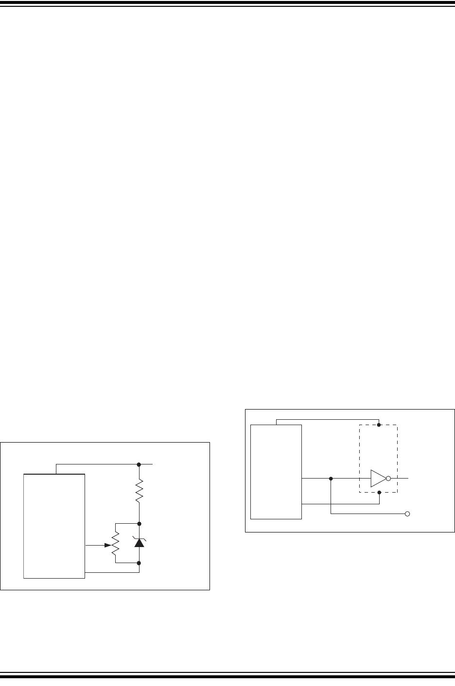
FIGURE 3-3: Simple Inverter for Fixed
Decimal Point
V+
V+
1.2V REF
COMMON
TC7116
TC7116A
TC7117
TC7117A
6.8kΩ
V
REF
+
20kΩ
TC7116
TC7116A
BP
TEST
37
21
V+
V+
GND
To LCD
Decimal
Point
To LCD
Backplane
4049

TC7117ACLW

Mfr. #:
Manufacturer:
Microchip Technology
Description:
LED Display Drivers w/Hold
Lifecycle:
New from this manufacturer.
Delivery:
DHL FedEx Ups TNT EMS
Payment:
T/T Paypal Visa MoneyGram Western Union