LTC3630
10
3630fd
For more information www.linear.com/LTC3630
An internal 0.8ms soft-start function limits the ramp rate
of the output voltage on start-up to prevent excessive input
supply droop. If a longer ramp time and consequently less
supply droop is desired, a capacitor can be placed from
the SS pin to ground. The 5µA current that is sourced
out of this pin will create a smooth voltage ramp on the
capacitor. If this ramp rate is slower than the internal
0.8ms soft-start, then the output voltage will be limited
by the ramp rate on the SS pin instead. The internal and
external soft-start functions are reset on start-up and after
an undervoltage event on the input supply.
The peak inductor current is not limited by the internal or
external soft-start functions; however, placing a capacitor
from the I
SET
pin to ground does provide this capability.
Peak Inductor Current Programming
The peak current comparator nominally limits the peak
inductor current to 1.2A. This peak inductor current can
be adjusted by placing a resistor from the I
SET
pin to
ground. The 5µA current sourced out of this pin through
the resistor generates a voltage that adjusts the peak cur
-
rent comparator threshold.
During sleep mode, the current sourced out of the I
SET
pin
is reduced to 1µA. The I
SET
current is increased back to 5µA
on the first switching cycle after exiting sleep mode. The
I
SET
current reduction in sleep mode, along with adding
a filtering capacitor, C
ISET
, from the I
SET
pin to ground,
provides a method of reducing light load output voltage
ripple at the expense of lower efficiency and slightly de
-
graded load step transient response.
For applications requiring higher output current, the
LTC3630 provides a feedback comparator output pin (FBO)
for combining the output current of multiple LTC3630s. By
connecting the FBO pin of a “master” LTC3630 to the V
FB
pin of one or more “slave” LTC3630s, the output currents
can be combined to source much more than 500mA.
operaTion
Dropout Operation
When the input supply decreases toward the output sup-
ply, the duty cycle increases to maintain regulation. The
P-channel MOSFET top switch in the L
TC3630 allows the
duty cycle to increase all the way to 100%. At 100% duty
cycle, the P-channel MOSFET stays on continuously
, pro
-
viding output current equal to the peak current, which can
be greater than 1A. The power dissipation of the LTC3630
can increase dramatically during dropout operation espe
-
cially at input voltages less than 10V
. The increased power
dissipation is due to higher potential output current and
increased P-channel MOSFET on-resistance. See the Ther
-
mal Considerations section of the Applications Information
for a detailed example.
Input Voltage and Overtemperature Protection
When using the LTC3630, care must be taken not to
exceed any of the ratings specified in the Absolute Maxi
-
mum Ratings section. As an added safeguard, however,
the L
TC3630 incorporates an overtemperature shutdown
feature. If the junction temperature reaches approximately
180°C, the L
TC3630 will enter thermal shutdown mode.
Both power switches will be turned off and the SW node
will become high impedance. After the part has cooled
below 160°C, it will restart. The overtemperature level is
not production tested.
The LTC3630 can provide a programmable undervoltage
lockout which can also serve as a precise input voltage
monitor by using a resistive divider from V
IN
to GND with
the tap connected to the RUN pin. Switching is enabled
when the RUN pin voltage exceeds 1.21V and is disabled
when dropping below 1.1V. Pulling the RUN pin below
700mV forces a low quiescent current shutdown (5µA).
Furthermore, if the input voltage falls below 3.5V typi
-
cal (3.7V maximum), an internal undervoltage detector
disables switching.
When switching is disabled, the LTC3630 can safely sus
-
tain input voltages up to the absolute maximum rating of
70V. Input supply undervoltage events trigger a soft-start
reset, which results in a graceful recovery from an input
supply transient.
(Refer to Block Diagram)
LTC3630
11
3630fd
For more information www.linear.com/LTC3630
applicaTions inForMaTion
The basic LTC3630 application circuit is shown on the front
page of the data sheet. External component selection is
determined by the maximum load current requirement and
begins with the selection of the peak current programming
resistor, R
ISET
. The inductor value L can then be determined,
followed by capacitors C
IN
and C
OUT
.
Peak Current Resistor Selection
The peak current comparator has a guaranteed current limit
of 1A (1.2A typical), which guarantees a maximum average
load current of 500mA. For applications that demand less
current, the peak current threshold can be reduced to as
little as 100mA (120mA typical). This lower peak current
allows the use of lower value, smaller components (input
capacitor, output capacitor, and inductor), resulting in
lower supply ripple and a smaller overall DC/DC converter.
The threshold can be easily programmed using a resis
-
tor (R
ISET
) between the I
SET
pin and ground. The voltage
generated on the I
SET
pin by R
ISET
and the internal 5µA
current source sets the peak current. The voltage on the
I
SET
pin is internally limited within the range of 0.1V to
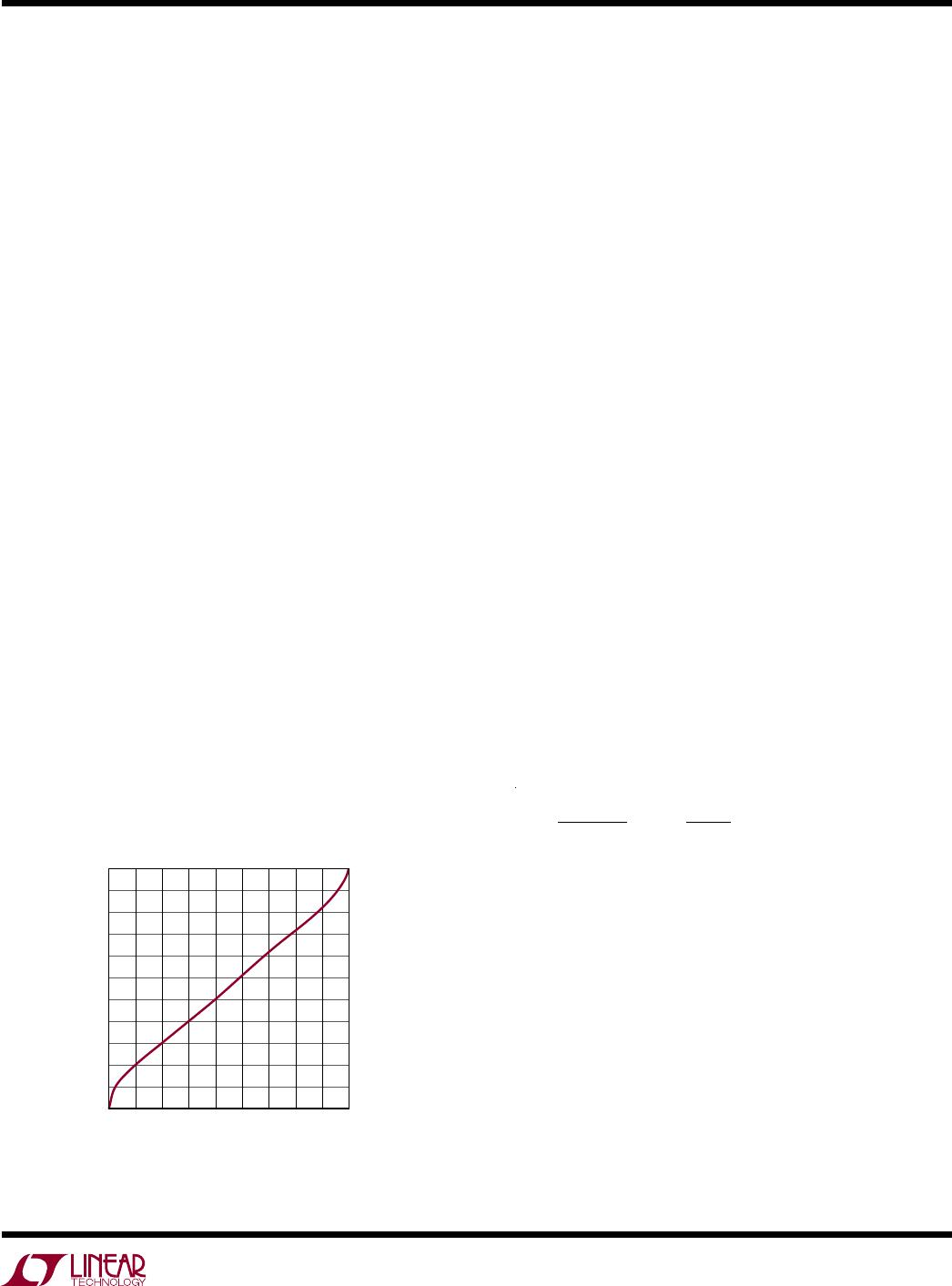
1.0V. The value of resistor for a particular peak current can
be selected by using Figure 2 or the following equation:
R
ISET
= I
PEAK
• 0.2 • 10
6
where 100mA < I
PEAK
< 1A.
The internal 5μA current source is reduced to 1μA in sleep
mode to maximize efficiency and to facilitate a trade-off
between efficiency and light load output voltage ripple, as
described in the C
ISET
Selection section of the Applica-
tions Information. For maximum efficiency, minimize the
capacitance on the I
SET
pin and place the R
ISET
resistor
as close to the pin as possible.
The typical peak current is internally limited to be within the
range of 120mA to 1.2A. Shorting the I
SET
pin to ground
programs the current limit to 120mA, and leaving it float
sets the current limit to the maximum value of 1.2A. When
selecting this resistor value, be aware that the maximum
average output current for this architecture is limited to
half of the peak current. Therefore, be sure to select a value
that sets the peak current with enough margin to provide
adequate load current under all conditions. Selecting the
peak current to be 2.2 times greater than the maximum
load current is a good starting point for most applications.
Inductor Selection
The inductor, input voltage, output voltage, and peak cur
-
rent determine the switching frequency during a burst
cycle of the LTC3630. For a given input voltage, output
voltage, and peak current, the inductor value sets the
switching frequency during a burst cycle when the output
is in regulation. Generally, switching between 50kHz and
250kHz yields high efficiency, and 200kHz is a good first
choice for many applications. The inductor value can be
determined by the following equation:
L =
V
OUT
f I
PEAK
1
V
OUT
V
IN
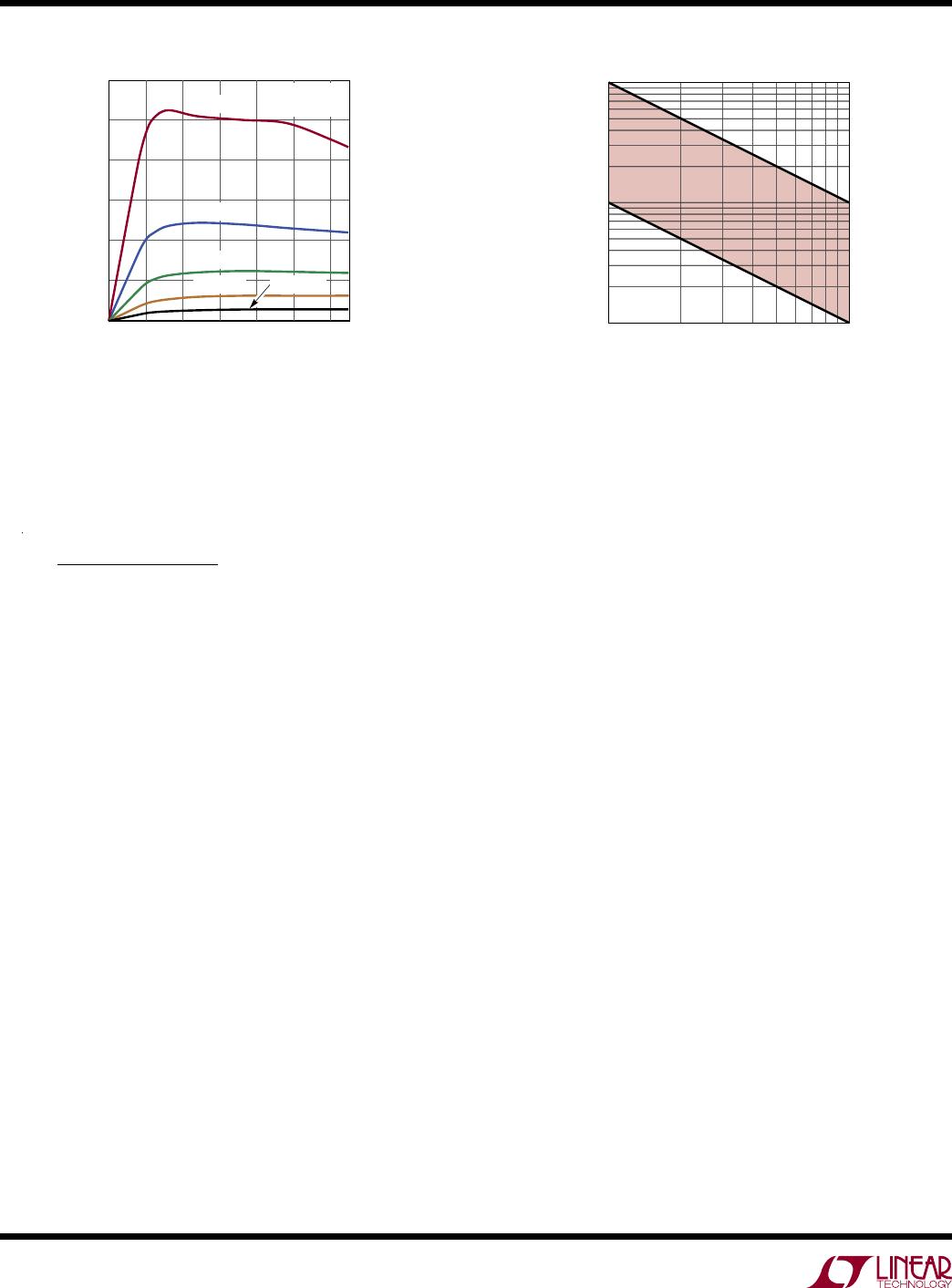
The variation in switching frequency during a burst cycle
with input voltage and inductance is shown in Figure 3. For
lower values of I
PEAK
, multiply the frequency in Figure3
by 1.2A/I
PEAK
.
An additional constraint on the inductor value is the
LTC3630’s 150ns minimum on-time of the high side switch.
Therefore, in order to keep the current in the inductor
Figure 2. R
ISET
Selection
MAXIMUM LOAD CURRENT (mA)
50
R
ISET
(kΩ)
60
180
200
220
150
250
300 350
3630 F02
20
140
100
40
160
0
120
80
100
200
400 450
500
LTC3630
12
3630fd
For more information www.linear.com/LTC3630
applicaTions inForMaTion
well-controlled, the inductor value must be chosen so that
it is larger than a minimum value which can be computed
as follows:
L >
V
IN(MAX)
t
ON(MIN)
I
PEAK
1.2
where V
IN(MAX)
is the maximum input supply voltage when
switching is enabled, t
ON(MIN)
is 150ns, I
PEAK
is the peak
current, and the factor of 1.2 accounts for typical inductor
tolerance and variation over temperature. Inductor values
that violate the above equation will cause the peak current
to overshoot and permanent damage to the part may occur.
Although the above equation provides the minimum in
-
ductor value, higher efficiency is generally achieved with
a larger inductor value, which produces a lower switching
frequency. The inductor value chosen should also be large
enough to keep the inductor current from going very nega
-
tive which is more of a concern at higher V
OUT
(>~12V). For
a given inductor type, however, as inductance is increased,
DC resistance (DCR) also increases. Higher DCR trans
-
lates into higher copper losses and lower current rating,
both of which place an upper limit on the inductance. The
recommended range of inductor values for small surface
mount inductors as a function of peak current is shown
in Figure 4. The values in this range are a good compromise
between the trade-offs discussed above. For applications
where board area is not a limiting factor, inductors with
l
arger cores can be used, which extends the recommended
range of Figure4 to larger values.
Inductor Core Selection
Once the value for L is known, the type of inductor must
be selected. High efficiency converters generally cannot
afford the core loss found in low cost powdered iron cores,
forcing the use of the more expensive ferrite cores. Actual
core loss is independent of core size for a fixed inductor
value but is very dependent of the inductance selected.
As the inductance increases, core losses decrease. Un
-
fortunately, increased inductance requires more turns of
wire and therefore copper losses will increase.
Ferrite designs have very low core losses and are pre
-
ferred at high switching frequencies, so design goals
can concentrate on copper loss and preventing satura-
tion. Ferrite core material saturates “hard,” which means
that
inductance collapses abruptly when the peak design
current is exceeded. This results in an abrupt increase in
inductor ripple current and consequently output voltage
ripple. Do not allow the core to saturate!
Figure 4. Recommended Inductor Values for Maximum Efficiency
Figure 3. Switching Frequency for V
OUT
= 3.3V
V
IN
INPUT VOLTAGE (V)
0
SWITCHING FREQUENCY (kHz)
400
500
600
60
3630 F03
300
200
0
10
20 30 40 50
100
V
OUT
= 3.3V
I
SET
OPEN
L = 4.2µH
L = 10µH
L = 22µH
L = 47µH L = 100µH
PEAK INDUCTOR CURRENT (mA)
100
10
INDUCTOR VALUE (µH)
100
1000
1000
3630 F04

LTC3630HDHC#PBF

Mfr. #:
Manufacturer:
Analog Devices / Linear Technology
Description:
Switching Voltage Regulators High Efficiency, 65V 500mA Synchronous Step-Down Converter
Lifecycle:
New from this manufacturer.
Delivery:
DHL FedEx Ups TNT EMS
Payment:
T/T Paypal Visa MoneyGram Western Union