LTC3630
16
3630fd
For more information www.linear.com/LTC3630
applicaTions inForMaTion
The RUN pin can alternatively be configured as a precise
undervoltage (UVLO) lockout on the V
IN
supply with a
resistive divider from V
IN
to ground. A simple resistive
divider can be used as shown in Figure 9 to meet specific
V
IN
voltage requirements.
Soft-Start
Soft-start is implemented by ramping the effective refer-
ence voltage from 0V to 0.8V. To increase the duration of
soft-start, place a capacitor from the SS pin to ground.
An internal 5µA pull-up current will charge this
capacitor.
The value of the soft-start capacitor can be calculated by
the following equation:
C
SS
= Soft-Start Time
5µA
0.35V
The minimum soft-start time is limited to the internal soft-
start timer of 0.8ms. When the LTC3630 detects a fault
condition (input supply undervoltage or overtemperature)
or when the RUN pin falls below 1.1V, the SS pin is quickly
pulled to ground and the internal soft-start timer is reset.
This ensures an orderly restart when using an external
soft-start capacitor.
Note that the soft-start capacitor may not be the limiting
factor in the output voltage ramp. The maximum output
current, which is equal to half the peak current, must
charge the output capacitor from 0V to its regulated value.
For small peak currents or large output capacitors, this
ramp time can be significant. Therefore, the output voltage
ramp time from 0V to the regulated V
OUT
value is limited
to a minimum of:
Ramp Time
2 C
OUT
I
PEAK
V
OUT
C
ISET
Selection
Once the peak current resistor, R
ISET
, and inductor are se-
lected to meet the load current and frequency requirements,
an optional capacitor, C
ISET
, can be added in parallel with
R
ISET
. This will boost efficiency at mid-loads and reduce
the output voltage ripple dependency on load current at the
expense of slightly degraded load step transient response.
The peak inductor current is controlled by the voltage on
the I
SET
pin. Current out of the I
SET
pin is 5µA while the
LTC3630 is switching and is reduced to 1µA during sleep
mode. The I
SET
current will return to 5µA on the first cycle
after sleep mode. Placing a parallel RC from the I
SET
pin to
ground filters the I
SET
voltage as the LTC3630 enters and
exits sleep mode which in turn will affect the output volt-
age ripple, efficiency and load step transient performance.
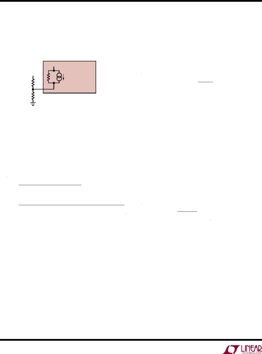
Figure 9. Adjustable UV Lockout
RUN
5V
2M
SLEEP, ACTIVE: 2µA
SHUTDOWN: 0µA
3630 F09
R3
V
IN
LTC3630
R4
The current that flows through the R3-R4 divider will
directly add to the shutdown, sleep, and active current
of the LTC3630, and care should be taken to minimize
the impact of this current on the overall efficiency of the
application circuit. To keep the variation of the rising V
IN
UVLO threshold to less than 5% due to the internal pull-
up circuitry, the following equations should be used to
calculate R3 and R4:
R3
RisingV
IN
UVLOThreshold
40µA
R4 =
R3 1.21V
RisingV
IN
UVLOThreshold 1.21V +R3 4µA
The falling UVLO threshold will be about 10% lower than
the rising V
IN
UVLO threshold due to the 110mV hysteresis
of the RUN comparator.
For applications that do not require a precise UVLO, the
RUN pin can be left floating. In this configuration, the UVLO
threshold is limited to the internal V
IN
UVLO thresholds as
shown in the Electrical Characteristics table.
Be aware that the RUN pin cannot be allowed to exceed
its absolute maximum rating of 6V. To keep the voltage
on the RUN pin from exceeding 6V, the following relation
should be satisfied:
V
IN(MAX)
< 4.5 • Rising V
IN
UVLO Threshold
To support a V
IN(MAX)
greater than 4.5x the external UVLO
threshold, an external 4.7V Zener diode should be used
in parallel with R4. See Figure 11.
LTC3630
17
3630fd
For more information www.linear.com/LTC3630
applicaTions inForMaTion
In general, when R
ISET
is greater than 120k a C
ISET
ca-
pacitor in the 100pF to 200pF range will improve most
performance parameters. When R
ISET
is less than 100k,
the capacitance on the I
SET
pin should be minimized.
Higher Current Applications
For applications that require more than 500mA, the
LTC3630 provides a feedback comparator output pin
(FBO) for driving additional LTC3630s. When the FBO pin
of a “master” LTC3630 is connected to the V
FB
pin of one
or more “slave” LTC3630s, the master controls the burst
cycle of the slaves.
Figure 10 shows an example of a 5V, 1A regulator using
two LTC3630s. The master is configured for a 5V fixed
output with external soft-start and the V
IN
UVLO level is
set by the RUN pin. Since the slaves are directly controlled
by the master, the SS pin of the slave should have minimal
capacitance and the RUN pin of the slave should be floating.
Furthermore, slaves should be configured for a 1.8V fixed
output (V
PRG1
= V
PRG2
= SS) to set the V
FB
pin threshold at
1.8V. The inductors L1 and L2 do not necessarily have to
be the same, but should both meet the criteria described
above in the Inductor Selection section.
Efficiency Considerations
The efficiency of a switching regulator is equal to the output
power divided by the input power times 100%. It is often
useful to analyze individual losses to determine what is
limiting the efficiency and which change would produce
the most improvement. Efficiency can be expressed as:
Efficiency = 100% – (L1 + L2 + L3 + ...)
where L1, L2, etc. are the individual losses as a percent
-
age of input power.
Although
all
dissipative elements in the circuit produce
losses, two main sources usually account for most of
the losses: V
IN
operating current and I
2
R losses. The V
IN
operating current dominates the efficiency loss at very
low load currents whereas the I
2
R loss dominates the
efficiency loss at medium to high load currents.
1. The V
IN
operating current comprises two components:
The DC supply current as given in the electrical charac-
teristics and the internal MOSFET gate charge currents.
The gate charge current results from switching the gate
capacitance of the internal power MOSFET switches.
Each time the gate is switched from high to low to
high again, a packet of charge,
Q, moves from V
IN
to
ground. The resulting Q/dt is the current out of V
IN
that is typically larger than the DC bias current.
2. I
2
R losses are calculated from the resistances of the
internal switches, R
SW
and external inductor R
L
. When
switching, the average output current flowing through
the inductor is “chopped” between the high side PMOS
switch and the low side NMOS switch. Thus, the series
resistance looking back into the switch pin is a function
of the top and bottom switch R
DS(ON)
values and the
duty cycle (DC = V
OUT
/V
IN
) as follows:
R
SW
= (R
DS(ON)TOP
)DC + (R
DS(ON)BOT
) • (1 – DC)
The R
DS(ON)
for both the top and bottom MOSFETs can
be obtained from the Typical Performance Characteris-
tics curves. Thus, to obtain the I
2
R losses, simply add
V
FB
SW
L1
L2
V
IN
RUN
R3
C
IN
C
OUT
V
OUT
5V
1A
C
SS
V
IN
R4
SS
V
PRG1
V
PRG2
FBO
LTC3630
(MASTER)
SW
V
FB
V
IN
RUN
SS
V
PRG1
V
PRG2
FBO
3630 F10
LTC3630
(SLAVE)
I
SET
I
SET
Figure 10. 5V, 1A Regulator
LTC3630
18
3630fd
For more information www.linear.com/LTC3630
applicaTions inForMaTion
R
SW
to R
L
and multiply the result by the square of the
average output current:
I
2
R Loss = I
O
2
(R
SW
+ R
L
)
Other losses, including C
IN
and C
OUT
ESR dissipative
losses and inductor core losses, generally account for
less than 2% of the total power loss.
Thermal Considerations
In most applications, the LTC3630 does not dissipate much
heat due to its high efficiency. But, in applications where
the LTC3630 is running at high ambient temperature with
low supply voltage and high duty cycles, such as dropout,
the heat dissipated may exceed the maximum junction
temperature of the part.
To prevent the LTC3630 from exceeding the maximum
junction temperature, the user will need to do some thermal
analysis. The goal of the thermal analysis is to determine
whether the power dissipated exceeds the maximum junc
-
tion temperature of the part. The temperature rise from
ambient to junction is given by:
T
R
= P
D
θ
JA
where P
D
is the power dissipated by the regulator and θ
JA
is the thermal resistance from the junction of the die to
the ambient temperature.
The junction temperature is given by:
T
J
= T
A
+ T
R
Generally, the worst-case power dissipation is in dropout
at low input voltage. In dropout, the LTC3630 can provide
a DC current as high as the full 1.2A peak current to the
output. At low input voltage, this current flows through a
higher resistance MOSFET, which dissipates more power.
As an example, consider the LTC3630 in dropout at an input
voltage of 5V, a load current of 500mA and an ambient
temperature of 85°C. From the Typical Performance graphs
of Switch On-Resistance, the R
DS(ON)
of the top switch
at V
IN
= 5V and 100°C is approximately 1.9Ω. Therefore,
the power dissipated by the part is:
P
D
= (I
LOAD
)
2
• R
DS(ON)
= (500mA)
2
• 1.9Ω = 0.475W
For the MSOP package the θ
JA
is 45°C/W. Thus, the junc-
tion temperature of the regulator is:
T
J
= 85°C+ 0.475W
45°C
W
= 106.4°C
which is below the maximum junction temperature of
150°C.
Note that the while the LTC3630 is in dropout, it can provide
output current that is equal to the peak current of the part.
This can increase the chip power dissipation dramatically
and may cause the internal overtemperature protection
circuitry to trigger at 180°C and shut down the LTC3630.
Design Example
As a design example, consider using the LTC3630 in an
application with the following specifications: typical V
IN
= 24V, maximum applied V
IN
= 70V, V
OUT
= 3.3V, I
OUT
=
500mA, f = 200kHz. Furthermore, assume for this example
that switching should start when V
IN
is greater than 12V.
First, calculate the inductor value that gives the required
switching frequency:
L =
3.3V
200kHz 1.2A
1
3.3V
24V
10µH
Next, verify that this value meets the L
MIN
requirement.
For this input voltage and peak current, the minimum
inductor value is:
L
MIN
=
24V 150ns
1.2A 1.2
= 2.5µH
Therefore, the minimum inductor requirement is satisfied
and the 10μH inductor value may be used.
Next, C
IN
and C
OUT
are selected. For this design, C
IN
should
be sized for a current rating of at least:
I
RMS
= 500mA
3.3V
24V
24V
3.3V
1 175mA
RMS

LTC3630HDHC#PBF

Mfr. #:
Manufacturer:
Analog Devices / Linear Technology
Description:
Switching Voltage Regulators High Efficiency, 65V 500mA Synchronous Step-Down Converter
Lifecycle:
New from this manufacturer.
Delivery:
DHL FedEx Ups TNT EMS
Payment:
T/T Paypal Visa MoneyGram Western Union