To reduce the electrical load on the host memory controller's command, address, and
control bus, Micron's RDIMMs utilize a DDR4 registering clock driver (RCD). The RCD
presents a single load to the controller while redriving signals to the DDR4 SDRAM de-
vices, which helps enable higher densities and increase signal integrity. The RCD also
provides a low-jitter, low-skew PLL that redistributes a differential clock pair to multiple
differential pairs of clock outputs.
Control Words
The RCD device(s) used on DDR4 RDIMMs, LRDIMMs, and NVDIMMs contain configu-
ration registers known as control words, which the host uses to configure the RCD
based on criteria determined by the module design. Control words can be set by the
host controller through either the DRAM address and control bus or the I
2
C bus inter-
face. The RCD I
2
C bus interface resides on the same I
2
C bus interface as the module
temperature sensor and EEPROM.
Parity Operations
The RCD includes a parity-checking function that can be enabled or disabled in control
word RC0E. The RCD receives a parity bit at the DPAR input from the memory control-
ler and compares it with the data received on the qualified command and address in-
puts; it indicates on its open-drain ALERT_n pin whether a parity error has occurred. If
parity checking is enabled, the RCD forwards commands to the SDRAM when no parity
error has occurred. If the parity error function is disabled, the RCD forwards sampled
commands to the SDRAM regardless of whether a parity error has occurred. Parity is al-
so checked during control word WRITE operations unless parity checking is disabled.
Rank Addressing
The chip select pins (CS_n) on Micron's modules are used to select a specific rank of
DRAM. The RDIMM is capable of selecting ranks in one of three different operating
modes, dependant on setting DA[1:0] bits in the DIMM configuration control word lo-
cated within the RCD. Direct DualCS mode is utilized for single- or dual-rank modules.
For quad-rank modules, either direct or encoded QuadCS mode is used.
16GB (x72, ECC, DR) 288-Pin DDR4 RDIMM
Registering Clock Driver Operation
09005aef862e760f
asf18c2gx72pdz.pdf - Rev. D 8/16 EN
10
Micron Technology, Inc. reserves the right to change products or specifications without notice.
© 2015 Micron Technology, Inc. All rights reserved.
Temperature Sensor with SPD EEPROM Operation
Thermal Sensor Operations
The integrated thermal sensor continuously monitors the temperature of the module
PCB directly below the device and updates the temperature data register. Temperature
data may be read from the bus host at any time, which provides the host real-time feed-
back of the module's temperature. Multiple programmable and read-only temperature
registers can be used to create a custom temperature-sensing solution based on system
requirements and JEDEC JC-42.2.
EVENT_n Pin
The temperature sensor also adds the EVENT_n pin (open-drain), which requires a pull-
up to V
DDSPD
. EVENT_n is a temperature sensor output used to flag critical events that
can be set up in the sensor’s configuration registers. EVENT_n is not used by the serial
presence-detect (SPD) EEPROM.
EVENT_n has three defined modes of operation: interrupt, comparator, and TCRIT. In
interrupt mode, the EVENT_n pin remains asserted until it is released by writing a 1 to
the clear event bit in the status register. In comparator mode, the EVENT_n pin clears
itself when the error condition is removed. Comparator mode is always used when the
temperature is compared against the TCRIT limit. In TCRIT only mode, the EVENT_n
pin is only asserted if the measured temperature exceeds the TCRIT limit; it then re-
mains asserted until the temperature drops below the TCRIT limit minus the TCRIT
hysteresis.
SPD EEPROM Operation
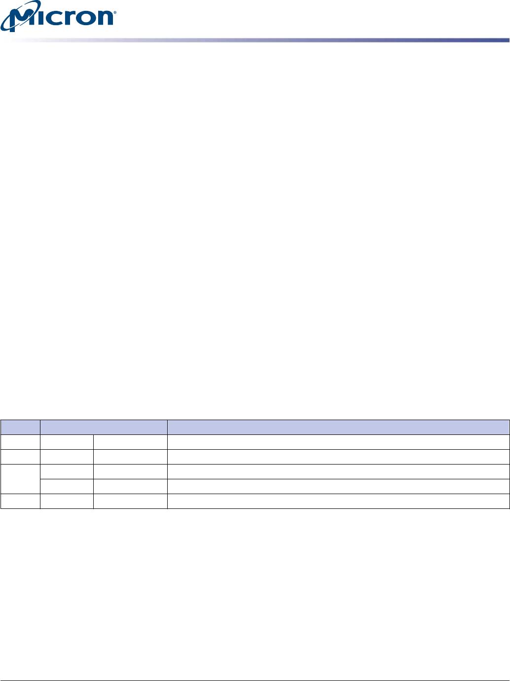
DDR4 SDRAM modules incorporate SPD. The SPD data is stored in a 512-byte, JEDEC
JC-42.4-compliant EEPROM that is segregated into four 128-byte, write-protectable
blocks. The SPD content is aligned with these blocks as shown in the table below.
Block Range Description
0 0–127 000h–07Fh Configuration and DRAM parameters
1 128–255 080h–0FFh Module parameters
2 256–319 100h–13Fh Reserved (all bytes coded as 00h)
320–383 140h–17Fh Manufacturing information
3 384–511 180h–1FFh End-user programmable
The first 384 bytes are programmed by Micron to comply with JEDEC standard JC-45,
"Appendix X: Serial Presence Detect (SPD) for DDR4 SDRAM Modules." The remaining
128 bytes of storage are available for use by the customer.
The EEPROM resides on a two-wire I
2
C serial interface and is not integrated with the
memory bus in any manner. It operates as a slave device in the I
2
C bus protocol, with all
operations synchronized by the serial clock. Transfer rates of up to 1 MHz are achieva-
ble at 2.5V (NOM).
Micron implements reversible software write protection on DDR4 SDRAM-based mod-
ules. This prevents the lower 384 bytes (bytes 0 to 383) from being inadvertently pro-
grammed or corrupted. The upper 128 bytes remain available for customer use and are
unprotected.
16GB (x72, ECC, DR) 288-Pin DDR4 RDIMM
Temperature Sensor with SPD EEPROM Operation
09005aef862e760f
asf18c2gx72pdz.pdf - Rev. D 8/16 EN
11
Micron Technology, Inc. reserves the right to change products or specifications without notice.
© 2015 Micron Technology, Inc. All rights reserved.
Electrical Specifications
Stresses greater than those listed may cause permanent damage to the module. This is a
stress rating only, and functional operation of the module at these or any other condi-
tions outside those indicated in each device's data sheet is not implied. Exposure to ab-
solute maximum rating conditions for extended periods may adversely affect reliability.
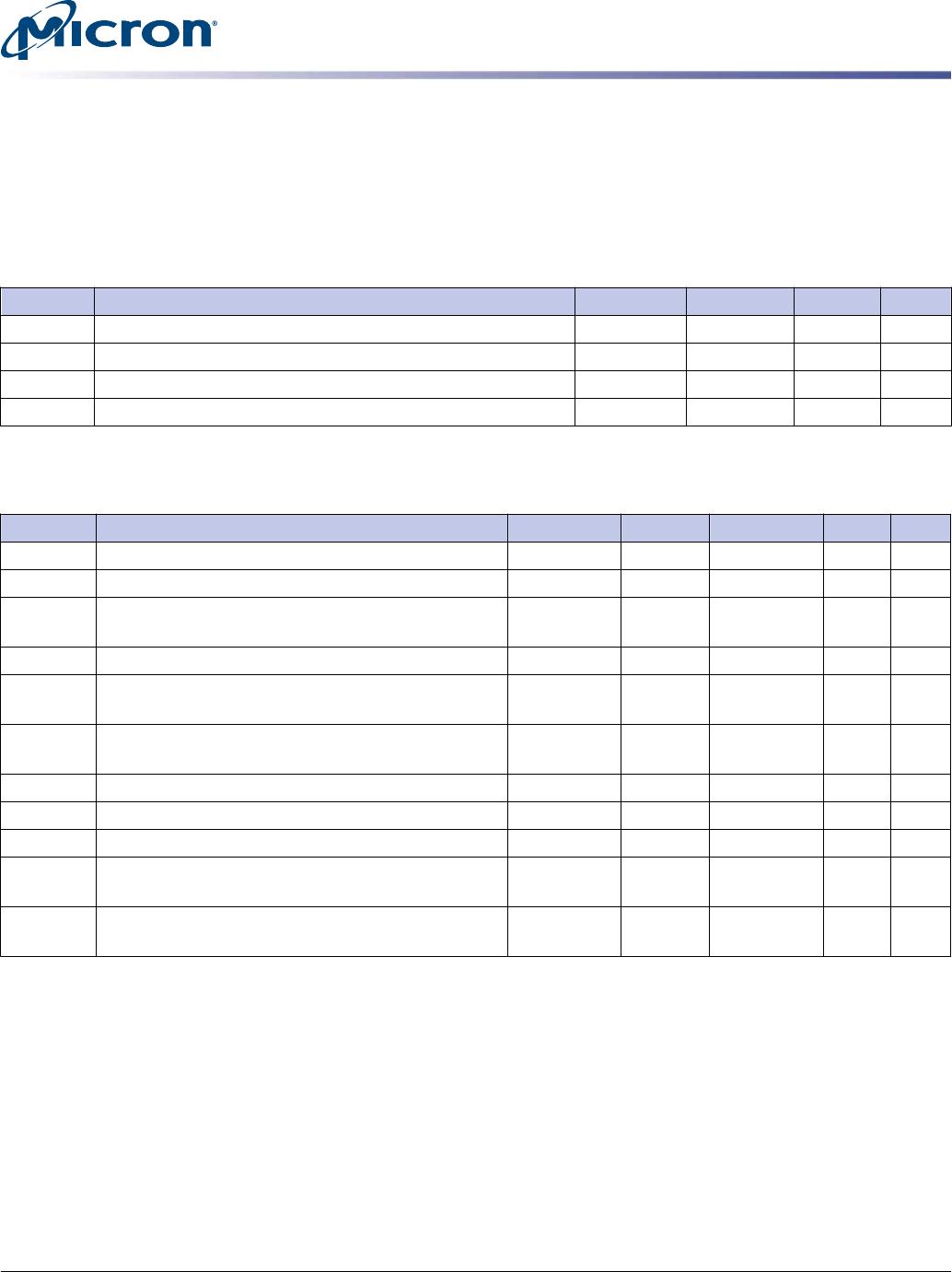
Table 8: Absolute Maximum Ratings
Symbol Parameter Min Max Units Notes
V
DD
V
DD
supply voltage relative to V
SS
–0.4 1.5 V 1
V
DDQ
V
DDQ
supply voltage relative to V
SS
–0.4 1.5 V 1
V
PP
Voltage on V
PP
pin relative to V
SS
–0.4 3.0 V 2
V
IN
, V
OUT
Voltage on any pin relative to V
SS
–0.4 1.5 V
Table 9: Operating Conditions
Symbol Parameter Min Nom Max Units Notes
V
DD
V
DD
supply voltage 1.14 1.20 1.26 V 1
V
PP
DRAM activating power supply 2.375 2.5 2.75 V 2
V
REFCA(DC)
Input reference voltage –
command/address bus
0.49 × V
DD
0.5 × V
DD
0.51 × V
DD
V 3
I
VTT
Termination reference current from V
TT
–750 750 mA
V
TT
Termination reference voltage (DC) –
command/address bus
0.49 × V
DD
-
20mV
0.5 × V
DD
0.51 × V
DD
+
20mV
V 4
I
IN
Input leakage current; any input excluding ZQ; 0V <
V
IN
< 1.1V
–2 2 µA 5
I
ZQ
Input leakage current; ZQ –3 3 µA 6, 7
I
I/O
DQ leakage; 0V < V
IN
< V
DD
–4 4 µA 7
I
OZpd
Output leakage current; V
OUT
= V
DD
; DQ is disabled 5 µA
I
OZpu
Output leakage current; V
OUT
= V
SS
; DQ and ODT
are disabled; ODT is disabled with ODT input HIGH
50 µA
I
VREFCA
V
REFCA
leakage; V
REFCA
= V
DD
/2 (after DRAM is ini-
tialized)
–2 2 µA 7
Notes:
1. V
DDQ
balls on DRAM are tied to V
DD
.
2. V
PP
must be greater than or equal to V
DD
at all times.
3. V
REFCA
must not be greater than 0.6 × V
DD
. When V
DD
is less than 500mV, V
REF
may be
less than or equal to 300mV.
4. V
TT
termination voltages in excess of specification limit adversely affect command and
address signals' voltage margins and reduce timing margins.
5. Command and address inputs are terminated to V
DD
/2 in the registering clock driver. In-
put current is dependent on termination resistance set in the registering clock driver.
6. Tied to ground. Not connected to edge connector.
7. Multiply by number of DRAM die on module.
16GB (x72, ECC, DR) 288-Pin DDR4 RDIMM
Electrical Specifications
09005aef862e760f
asf18c2gx72pdz.pdf - Rev. D 8/16 EN
12
Micron Technology, Inc. reserves the right to change products or specifications without notice.
© 2015 Micron Technology, Inc. All rights reserved.

MTA18ASF2G72PDZ-2G3D1

Mfr. #:
Manufacturer:
Micron
Description:
Memory Modules DDR4 16GB RDIMM
Lifecycle:
New from this manufacturer.
Delivery:
DHL FedEx Ups TNT EMS
Payment:
T/T Paypal Visa MoneyGram Western Union