Functional Block Diagram
Figure 2: Functional Block Diagram
DQ
DQ
DQ
DQ
DQ
DQ
DQ
DQ
ZQ
DQ0
DQ1
DQ2
DQ3
DQ4
DQ5
DQ6
DQ7
U2
DQ
DQ
DQ
DQ
DQ
DQ
DQ
DQ
U20
DQ32
DQ33
DQ34
DQ35
DQ36
DQ37
DQ38
DQ39
U8
DQ
DQ
DQ
DQ
DQ
DQ
DQ
DQ
U15
DQ8
DQ9
DQ10
DQ11
DQ12
DQ13
DQ14
DQ15
U3
DQ
DQ
DQ
DQ
DQ
DQ
DQ
DQ
U19
DQ40
DQ41
DQ42
DQ43
DQ44
DQ45
DQ46
DQ47
U9
DQ
DQ
DQ
DQ
DQ
DQ
DQ
DQ
U14
DQ16
DQ17
DQ18
DQ19
DQ20
DQ21
DQ22
DQ23
U4
DQ
DQ
DQ
DQ
DQ
DQ
DQ
DQ
U18
DQ48
DQ49
DQ50
DQ51
DQ52
DQ53
DQ54
DQ55
U10
DQ
DQ
DQ
DQ
DQ
DQ
DQ
DQ
U13
DQ24
DQ25
DQ26
DQ27
DQ28
DQ29
DQ30
DQ31
U5
DQ
DQ
DQ
DQ
DQ
DQ
DQ
DQ
U17
DQ56
DQ57
DQ58
DQ59
DQ60
DQ61
DQ62
DQ63
U11
DQ
DQ
DQ
DQ
DQ
DQ
DQ
DQ
U12
CB0
CB1
CB2
CB3
CB4
CB5
CB6
CB7
U6
DQ
DQ
DQ
DQ
DQ
DQ
DQ
DQ
U16
DQ
DQ
DQ
DQ
DQ
DQ
DQ
DQ
ZQ
DQ
DQ
DQ
DQ
DQ
DQ
DQ
DQ
ZQ
DQ
DQ
DQ
DQ
DQ
DQ
DQ
DQ
ZQ
DQ
DQ
DQ
DQ
DQ
DQ
DQ
DQ
ZQ
DQ
DQ
DQ
DQ
DQ
DQ
DQ
DQ
ZQ
DQ
DQ
DQ
DQ
DQ
DQ
DQ
DQ
ZQ
DQ
DQ
DQ
DQ
DQ
DQ
DQ
DQ
ZQ
DQ
DQ
DQ
DQ
DQ
DQ
DQ
DQ
ZQ
CS1_n
CS0_n
Vss
Vss
Vss
Vss
Vss
Vss
Vss
Vss
Vss
ZQ
Vss
ZQ
Vss
ZQ
Vss
ZQ
Vss
ZQ
Vss
ZQ
ZQ
Vss
ZQ
Vss
ZQ
Vss
DM_n/ CS_n DQS_t DQS_c
DBI_n
DQS0_t
DQS0_c
DBI0_n/DM0_n
DM_n/ CS_n DQS_t DQS_c
DBI_n
DM_n/ CS_n DQS_t DQS_c
DBI_n
DM_n/ CS_n DQS_t DQS_c
DBI_n
DM_n/ CS_n DQS_t DQS_c
DBI_n
DM_n/ CS_n DQS_t DQS_c
DBI_n
DM_n/ CS_n DQS_t DQS_c
DBI_n
DM_n/ CS_n DQS_t DQS_c
DBI_n
DM_n/ CS_n DQS_t DQS_c
DBI_n
DM_n/ CS_n DQS_t DQS_c
DBI_n
DM_n/ CS_n DQS_t DQS_c
DBI_n
DM_n/ CS_n DQS_t DQS_c
DBI_n
DM_n/ CS_n DQS_t DQS_c
DBI_n
DM_n/ CS_n DQS_t DQS_c
DBI_n
DM_n/ CS_n DQS_t DQS_c
DBI_n
DM_n/ CS_n DQS_t DQS_c
DBI_n
DM_n/ CS_n DQS_t DQS_c
DBI_n
DM_n/ CS_n DQS_t DQS_c
DBI_n
DQS1_t
DQS1_c
DBI1_n/DM1_n
DQS2_t
DQS2_c
DBI2_n/DM2_n
DQS3_t
DQS3_c
DBI3_n/DM3_n
DQS8_t
DQS8_c
DBI8_n/DM8_n
DQS4_t
DQS4_c
DBI4_n/DM4_n
DQS5_t
DQS5_c
DBI5_n/DM5_n
DQS6_t
DQS6_c
DBI6_n/DM6_n
DQS7_t
DQS7_c
DBI7_n/DM7_n
U7
A/B-CS_n[1:0], A/B-BA[1:0]A/B-BG[1:0],
A/B-ACT_n, A/B-A[17, 13:0], A/B-RAS_n/A16,
A/B-CAS_n/A15, A/B-WE_n/A14,
A/B-PAR, A/B-CKE[1:0], A/B-ODT[1:0]
CK[3:0]_t
CK[3:0]_c
Command, control, address, and clock line terminations:
DDR4
SDRAM
VTT
DDR4
SDRAM
VDD
U1
A0
SPD EEPROM/
Temperature
sensor
A1 A2
SA0
SA1
SDA
SCL
EVT
EVENT#
SA2
Rank 0: U2–U6, U8–U11
Rank 1: U12–U20
CKNC_t
CKNC_c
Vss
VREFCA
VSS
DDR4 SDRAM, Register
VDD
Control, command and
address termination
VDDSPD
SPD EEPROM/Temp Sensor,
Register
VTT
DDR4 SDRAM, Register
DDR4 SDRAM
VPP
CS0_n
CS1_n
BA[1:0]
BG[1:0]
ACT_n
A[17, 13:0]
RAS_n/A16
CAS_n/A15
WE_n/A14
CKE0
CKE1
ODT0
ODT1
PAR_IN
ALERT_CONN
A/BCS0_n: Rank 0
A/BCS1_n: Rank 1
A/BBA[1:0]: DDR4 SDRAM
A/BBG[1:0]: DDR4 SDRAM
A/BACT_n: DDR4 SDRAM
A/BA[17,13:0]: DDR4 SDRAM
A/B-RAS_n/A16: DDR4 SDRAM
A/B-CAS_n/A15: DDR4 SDRAM
A/B-WE_n/A14: DDR4 SDRAM
A/BCKE0: Rank 0
A/BCKE1: Rank 1
A/BODT0: Rank 0
A/BODT1: Rank 1
A/BPAR: DDR4 SDRAM
ALERT_DRAM: DDR4 SDRAM
R
E
G
I
S
T
E
R
&
P
L
L
RESET_CONN
CK_t
CK_c
CK[1:0]_c
DDR4 SDRAM
RESET_DRAM: DDR4 SDRAM
CK[1:0]_t
ZQ
VSS
SA0
SA1
SA2
SCL
SDA
Note:
1. The ZQ ball on each DDR4 component is connected to an external 240Ω ±1% resistor
that is tied to ground. It is used for the calibration of the component’s ODT and output
driver.
16GB (x72, ECC, DR) 288-Pin DDR4 RDIMM
Functional Block Diagram
09005aef862e760f
asf18c2gx72pdz.pdf - Rev. D 8/16 EN
7
Micron Technology, Inc. reserves the right to change products or specifications without notice.
© 2015 Micron Technology, Inc. All rights reserved.
General Description
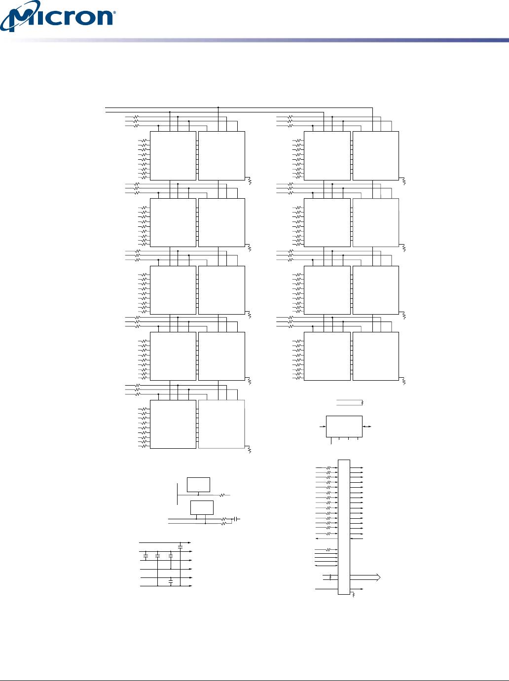
High-speed DDR4 SDRAM modules use DDR4 SDRAM devices with two or four internal
memory bank groups. DDR4 SDRAM modules utilizing 4- and 8-bit-wide DDR4 SDRAM
devices have four internal bank groups consisting of four memory banks each, provid-
ing a total of 16 banks. 16-bit-wide DDR4 SDRAM devices have two internal bank
groups consisting of four memory banks each, providing a total of eight banks. DDR4
SDRAM modules benefit from DDR4 SDRAM's use of an 8n-prefetch architecture with
an interface designed to transfer two data words per clock cycle at the I/O pins. A single
READ or WRITE operation for the DDR4 SDRAM effectively consists of a single 8n-bit-
wide, four-clock data transfer at the internal DRAM core and eight corresponding n-bit-
wide, one-half-clock-cycle data transfers at the I/O pins.
DDR4 modules use two sets of differential signals: DQS_t and DQS_c to capture data
and CK_t and CK_c to capture commands, addresses, and control signals. Differential
clocks and data strobes ensure exceptional noise immunity for these signals and pro-
vide precise crossing points to capture input signals.
Fly-By Topology
DDR4 modules use faster clock speeds than earlier DDR technologies, making signal
quality more important than ever. For improved signal quality, the clock, control, com-
mand, and address buses have been routed in a fly-by topology, where each clock, con-
trol, command, and address pin on each DRAM is connected to a single trace and ter-
minated (rather than a tree structure, where the termination is off the module near the
connector). Inherent to fly-by topology, the timing skew between the clock and DQS sig-
nals can be easily accounted for by using the write-leveling feature of DDR4.
Module Manufacturing Location
Micron Technology manufactures modules at sites world-wide. Customers may receive
modules from any of the following manufacturing locations:
Table 6: DRAM Module Manufacturing Locations
Manufacturing Site Location Country of Origin Specified on Label
Boise, USA USA
Aguadilla, Puerto Rico Puerto Rico
Xian, China China
Singapore Singapore
16GB (x72, ECC, DR) 288-Pin DDR4 RDIMM
General Description
09005aef862e760f
asf18c2gx72pdz.pdf - Rev. D 8/16 EN
8
Micron Technology, Inc. reserves the right to change products or specifications without notice.
© 2015 Micron Technology, Inc. All rights reserved.
Address Mapping to DRAM
Address Mirroring
To achieve optimum routing of the address bus on DDR4 multi rank modules, the ad-
dress bus will be wired as shown in the table below, or mirrored. For quad rank mod-
ules, ranks 1 and 3 are mirrored and ranks 0 and 2 are non-mirrored. Highlighted ad-
dress pins have no secondary functions allowing for normal operation when cross-
wired. Data is still read from the same address it was written. However, Load Mode op-
erations require a specific address. This requires the controller to accommodate for a
rank that is "mirrored." Systems may reference DDR4 SPD to determine if the module
has mirroring implemented or not. See the JEDEC DDR4 SPD specification for more de-
tails.
Table 7: Address Mirroring
Edge Connector Pin DRAM Pin, Non-mirrored DRAM Pin, Mirrored
A0 A0 A0
A1 A1 A1
A2 A2 A2
A3 A3 A4
A4 A4 A3
A5 A5 A6
A6 A6 A5
A7 A7 A8
A8 A8 A7
A9 A9 A9
A10 A10 A10
A11 A11 A13
A13 A13 A11
A12 A12 A12
A14 A14 A14
A15 A15 A15
A16 A16 A16
A17 A17 A17
BA0 BA0 BA1
BA1 BA1 BA0
BG0 BG0 BG1
BG1 BG1 BG0
Registering Clock Driver Operation
Registered DDR4 SDRAM modules use a registering clock driver device consisting of a
register and a phase-lock loop (PLL). The device complies with the JEDEC DDR4 RCD
specification.
16GB (x72, ECC, DR) 288-Pin DDR4 RDIMM
Address Mapping to DRAM
09005aef862e760f
asf18c2gx72pdz.pdf - Rev. D 8/16 EN
9
Micron Technology, Inc. reserves the right to change products or specifications without notice.
© 2015 Micron Technology, Inc. All rights reserved.

MTA18ASF2G72PDZ-2G3D1

Mfr. #:
Manufacturer:
Micron
Description:
Memory Modules DDR4 16GB RDIMM
Lifecycle:
New from this manufacturer.
Delivery:
DHL FedEx Ups TNT EMS
Payment:
T/T Paypal Visa MoneyGram Western Union