1 kV, Dual Channel Digital Isolators
Data Sheet
ADuM7240/ADuM7241
Rev. B
Document Feedback
Information furnished by Analog Devices is believed to be accurate and reliable. However, no
responsibility is assumed by Analog Devices for its use, nor for any infringements of patents or other
rights of third parties that may result from its use. Specifications subject to change without notice. No
license is granted by implication or otherwise under any patent or patent rights of Analog Devices.
Trademarks and registered trademarks are the property of their respective owners.
One Technology Way, P.O. Box 9106, Norwood, MA 02062-9106, U.S.A.
Tel: 781.329.4700 ©20122015 Analog Devices, Inc. All rights reserved.
Technical Support www.analog.com
FEATURES
Narrow-body, RoHS-compliant, 8-lead SOIC
Safety and regulatory approvals
UL recognition
UL 1577: 1000 V rms for 1 minute
Low power operation
5 V operation
2.4 mA per channel maximum at 0 Mbps to 1 Mbps
11.8 mA per channel maximum at 25 Mbps
3.3 V operation
1.7 mA per channel maximum at 0 Mbps to 1 Mbps
8.2 mA per channel maximum at 25 Mbps
Bidirectional communication
Up to 25 Mbps data rate (NRZ)
3 V/5 V level translation
High temperature operation: 105°C
High common-mode transient immunity: >15 kV/μs
APPLICATIONS
General-purpose multichannel isolation
Data converter isolation
Industrial field bus isolation
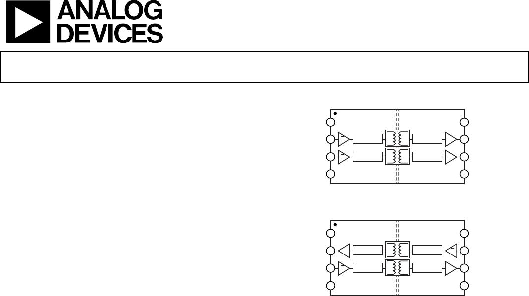
FUNCTIONAL BLOCK DIAGRAMS
ENCODE DECODE
ENCODE
DECODE
V
DD1
V
IA
V
IB
GND
1
V
DD2
V
OA
V
OB
GND
2
1
2
3
4
8
7
6
5
ADuM7240
10240-001
Figure 1. ADuM7240
ENCODE DECODE
DECODE
ENCODE
V
DD1
V
OA
V
IB
GND
1
V
DD2
V
IA
V
OB
GND
2
1
2
3
4
8
7
6
5
ADuM7241
10240-002
Figure 2. ADuM7241
GENERAL DESCRIPTION
The ADuM7240/ADuM7241
1
are dual channel digital isolators
based on the Analog Devices, Inc., iCoupler® technology.
Combining high speed CMOS and monolithic air core trans-
former technologies, these isolation components provide
outstanding performance characteristics superior to the alterna-
tives, such as optocoupler devices and other integrated couplers.
The ADuM7240/ADuM7241 dual 1 kV digital isolation devices
are packaged in a narrow-body 8-lead SOIC. The ADuM7240/
ADuM7241 offer a cost-effective option compared to 2.5 kV or
5 kV isolators where only functional isolation is needed.
Like other Analog Devices isolators, the ADuM7240/ADuM7241
offer very low power consumption, consuming one-tenth to
one-sixth the power of comparable isolators at data rates up to
25 Mbps. Despite the low power consumption, all models of the
ADuM7240/ADuM7241 provide low pulse width distortion
(<5 ns for C grade). In addition, every model has an input glitch
filter to protect against extraneous noise disturbances.
The ADuM7240/ADuM7241 provide two independent isolation
channels and are available in two channel configurations with
1 Mbps or 25 Mbps data rates (see the Ordering Guide). All
models operate with the supply voltage on either side ranging
from 3.0 V to 5.5 V, providing compatibility with lower voltage
systems as well as enabling voltage translation functionality
across the isolation barrier. The ADuM7240/ADuM7241 also
have an output default high logic state in the absence of input
power.
1
Protected by U.S. Patents 5,952,849; 6,873,065; and 7,075,329. Other patents pending.
ADuM7240/ADuM7241 Data Sheet
Rev. B | Page 2 of 16
TABLE OF CONTENTS
Features .............................................................................................. 1
Applications ....................................................................................... 1
Functional Block Diagrams ............................................................. 1
General Description ......................................................................... 1
Revision History ............................................................................... 2
Specifications ..................................................................................... 3
Electrical Characteristics5 V Operation................................ 3
Electrical Characteristics3.3 V Operation ............................ 4
Electrical CharacteristicsMixed 5 V/3.3 V Operation ........ 5
Electrical CharacteristicsMixed 3.3 V/5 V Operation ........ 6
Package Characteristics ............................................................... 7
Regulatory Information ............................................................... 7
Insulation and Safety-Related Specifications ............................ 7
Recommended Operating Conditions ...................................... 7
Absolute Maximum Ratings ............................................................8
ESD Caution...................................................................................8
Pin Configurations and Function Descriptions ............................9
Typical Performance Characteristics ........................................... 10
Applications Information .............................................................. 12
Printed Circuit Board Layout ................................................... 12
Propagation Delay-Related Parameters ................................... 12
DC Correctness .......................................................................... 12
Magnetic Field Immunity.......................................................... 12
Power Consumption .................................................................. 13
Insulation Lifetime ..................................................................... 13
Outline Dimensions ....................................................................... 14
Ordering Guide .......................................................................... 14
REVISION HISTORY
10/15Rev. A to Rev. B
Change to Features Section ............................................................. 1
Changes to Table 14 .......................................................................... 7
5/12Rev. 0 to Rev. A
Changes to Table 2 ............................................................................ 3
Changed I
DDI(Q)
Maximum Parameter from 1.2 mA to 1.4 mA,
Table 3, and I
DDO(Q)
Maximum Parameter from 0.95 mA to
1.1 mA, Table 3 ................................................................................. 3
Changes to Table 5 ............................................................................ 4
Changed I
DDI(Q)
Maximum Parameter from 0.83 mA to 1.0 mA,
Table 6, and Changed I
DDO(Q)
Maximum Parameter from
0.68 mA to 0.8 mA, Table 6 ............................................................. 4
Changes to Table 8 ............................................................................ 5
Changed I
DDI(Q)
Maximum Parameter from 1.2 mA to 1.45 mA,
Table 9, and Changed I
DDO(Q)
Maximum Parameter from
0.67 mA to 0.80 mA, Table 9 ........................................................... 5
Changes to Table 11 .......................................................................... 6
Changed I
DDI(Q)
Maximum Parameter from 0.83 mA to 1.0 mA,
Table 12, and Changed I
DDO(Q)
Maximum Parameter from
0.90 mA to 1.1 mA, Table 12 ........................................................... 6
5/12—Revision 0: Initial Version
Data Sheet ADuM7240/ADuM7241
Rev. B | Page 3 of 16
SPECIFICATIONS
ELECTRICAL CHARACTERISTICS5 V OPERATION
All typical specifications are at T
A
= 25°C, V
DD1
= V
DD2
= 5 V. Minimum/maximum specifications apply over the entire recommended
operation range of 4.5 V ≤ V
DD1
≤ 5.5 V, 4.5 V ≤ V
DD2
5.5 V, and −40°C T
A
+105°C, unless otherwise noted. Switching specifications
are tested with C
L
= 15 pF and CMOS signal levels, unless otherwise noted.
Table 1.
C Grade
Parameter Symbol Min Typ Max Min Typ Max Unit Test Conditions/Comments
SWITCHING SPECIFICATIONS
Pulse Width PW 250 40 ns Within PWD limit
Data Rate 1 25 Mbps Within PWD limit
Propagation Delay t
PHL
, t
PLH
50 75 32 41 50 ns 50% input to 50% output
Pulse Width Distortion PWD 10 25 2 5 ns |t
PLH
− t
PHL
|
Change vs. Temperature
5
3
ps/°C
Propagation Delay Skew
1
t
PSK
20 10 ns
Channel Matching
Codirectional t
PSKCD
25 2 4 ns
Opposing Direction t
PSKOD
30 2 6 ns
Jitter
2
2
ns
1
t
PSK
is the magnitude of the worst-case difference in t
PHL
or t
PLH
that is measured between units at the same operating temperature, supply voltages, and output load
within the recommended operating conditions.
Table 2.
1 Mbps—A, C Grades
25 MbpsC Grade
Parameter
Symbol
Min
Typ
Max
Min
Typ
Max
Unit
Test Conditions/Comments
SUPPLY CURRENT
ADuM7240 I
DD1
2.2 2.8 16 21 mA
I
DD2
1.7 2.2 3.9 5.7 mA
ADuM7241 I
DD1
1.9 2.4 9.3 13 mA
I
DD2
1.9 2.4 8.2 12 mA
Table 3. For All Models
Parameter Symbol Min Typ Max Unit Test Conditions/Comments
DC SPECIFICATIONS
Logic High Input Threshold V
IH
0.7 V
DDx
V
Logic Low Input Threshold V
IL
0.3 V
DDx
V
Logic High Output Voltages V
OH
V
DDx
− 0.1 V
DDx
V I
Ox
= −20 µA, V
Ix
= V
IxH
V
DDx
− 0.4 V
DDx
− 0.3 V I
Ox
= −4 mA, V
Ix
= V
IxH
Logic Low Output Voltages
V
OL
0.0
0.1
V
I
Ox
= 20 µA, V
Ix
= V
IxL
0.2 0.4 V I
Ox
= 4 mA, V
Ix
= V
IxL
Input Current per Channel I
I
−10
+0.01
+10
µA
0 V ≤ V
Ix
≤ V
DDx
Supply Current per Channel
Quiescent Input Supply Current I
DDI(Q)
1 1.4 mA
Quiescent Output Supply Current
I
DDO(Q)
0.8
1.1
mA
Dynamic Input Supply Current I
DDI(D)
0.29 mA/Mbps
Dynamic Output Supply Current I
DDO(D)
0.03 mA/Mbps
AC SPECIFICATIONS
Output Rise/Fall Time t
R
/t
F
2.0 ns 10% to 90%
Common-Mode Transient Immunity
1
|CM| 15 25 kV/µs V
Ix
= V
DDx
, V
CM
= 1000 V,
transient magnitude = 800 V
Refresh Rate f
r
600 kHz DC data inputs
1
|CM| is the maximum common-mode voltage slew rate that can be sustained while maintaining V
O
> 0.8 V
DDx
. The common-mode voltage slew rates apply to both
rising and falling common-mode voltage edges.

ADUM7240ARZ

Mfr. #:
Manufacturer:
Analog Devices Inc.
Description:
Digital Isolators 1kV Dual-CH Digital
Lifecycle:
New from this manufacturer.
Delivery:
DHL FedEx Ups TNT EMS
Payment:
T/T Paypal Visa MoneyGram Western Union