Data Sheet ADuM7240/ADuM7241
Rev. B | Page 7 of 16
PACKAGE CHARACTERISTICS
Table 13.
Parameter Symbol Min Typ Max Unit Test Conditions/Comments
Resistance (Input-to-Output)
1
R
I-O
10
13
Capacitance (Input-to-Output)
1
C
I-O
2 pF f = 1 MHz
Input Capacitance
2
C
I
4 pF
IC Junction-to-Ambient Thermal
Resistance
θ
JA
85 °C/W Thermocouple located at center of package
underside
1
The device is considered a 2-terminal device: Pin 1 through Pin 4 are shorted together, and Pin 5 through Pin 8 are shorted together.
2
Input capacitance is from any input data pin to ground.
REGULATORY INFORMATION
The ADuM7240/ADuM7241 are pending approval by the organizations listed in Table 14. See Table 18 and the Insulation Lifetime
section for recommended maximum working voltages for specific cross-isolation waveforms and insulation levels.
Table 14.
UL
Recognized Under UL 1577 Component Recognition Program
1
Single Protection, 1000 V rms Isolation Voltage
File E214100
1
In accordance with UL 1577, each ADuM7240/ADuM7241 is proof tested by applying an insulation test voltage ≥1200 V rms for 1 sec (current leakage detection limit = 5 µA).
INSULATION AND SAFETY-RELATED SPECIFICATIONS
Table 15.
Parameter Symbol Value Unit Test Conditions/Comments
Rated Dielectric Insulation Voltage 1000 V rms 1-minute duration
Minimum External Air Gap (Clearance) L(I01) 4.0 mm min Measured from input terminals to output terminals,
shortest distance through air
Minimum External Tracking (Creepage) L(I02) 4.0 mm min Measured from input terminals to output terminals,
shortest distance path along body
Minimum Internal Gap (Internal Clearance) 2.6 μm min Distance through insulation
Tracking Resistance (Comparative Tracking Index) CTI >175 V DIN IEC 112/VDE 0303 Part 1
Isolation Group IIIa Material Group (DIN VDE 0110, 1/89, Table 1)
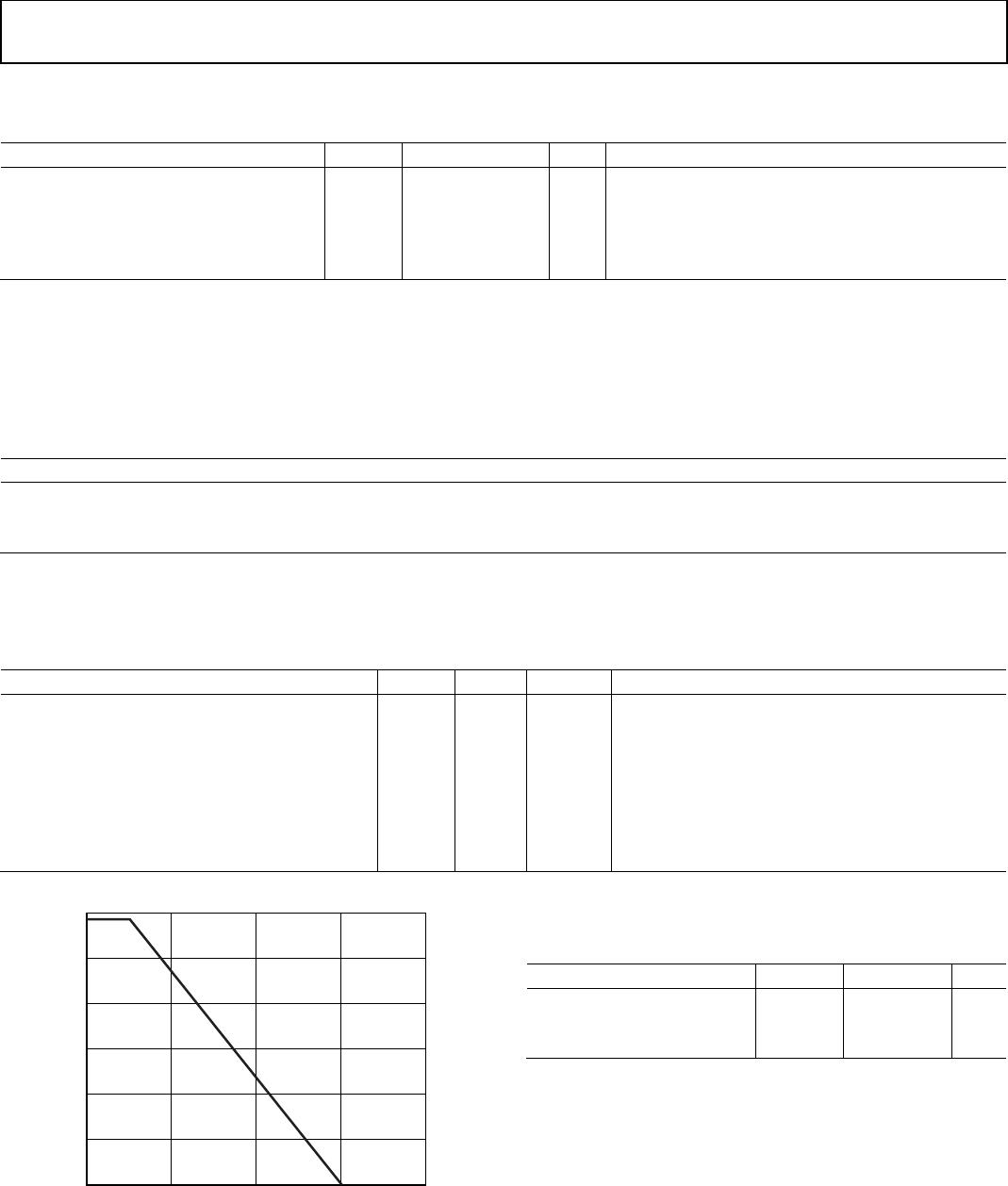
300
0
0 200
10240-003
SAFETY-LIMITING CURRENT (mA)
AMBIENT TEMPERATURE (°C)
250
200
150
100
50
50 100 150
Figure 3. Thermal Derating Curve, Dependence of Safety-Limiting Values
with Ambient Temperature per DIN V VDE V 0884-10
RECOMMENDED OPERATING CONDITIONS
Table 16.
Parameter Symbol Min Max Unit
Operating Temperature T
A
−40 +105 °C
Supply Voltages
1
V
DD1
, V
DD2
3.0 5.5 V
Input Signal Rise and Fall Times 1.0 ms
1
All voltages are relative to their respective ground. See the DC Correctness
section for information about immunity to external magnetic fields.
ADuM7240/ADuM7241 Data Sheet
Rev. B | Page 8 of 16
ABSOLUTE MAXIMUM RATINGS
T
A
= 25°C, unless otherwise noted.
Table 17.
Parameter Rating
Storage Temperature (T
ST
) Range −65°C to +150°C
Ambient Operating Temperature
(T
A
) Range
40°C to +105°C
Supply Voltages (V
DD1
, V
DD2
) −0.5 V to +7.0 V
Input Voltages (V
IA
, V
IB
)
1
−0.5 V to V
DDI
+ 0.5 V
Output Voltages (V
OA
, V
OB
)
1
−0.5 V to V
DDO
+ 0.5 V
Average Output Current per Pin
2
Side 1 (I
O1
) −10 mA to +10 mA
Side 2 (I
O2
) −10 mA to +10 mA
Common-Mode Transients
3
−100 kV/µs to +100 kV/µs
1
V
DDI
and V
DDO
refer to the supply voltages on the input and output sides of a
given channel, respectively. See the Printed Circuit Board Layout section.
2
See Figure 3 for maximum rated current values for various temperatures.
3
Refers to common-mode transients across the insulation barrier. Common-
mode transients exceeding the absolute maximum ratings may cause latch-
up or permanent damage.
Stresses at or above those listed under Absolute Maximum
Ratings may cause permanent damage to the product. This is a
stress rating only; functional operation of the product at these
or any other conditions above those indicated in the operational
section of this specification is not implied. Operation beyond
the maximum operating conditions for extended periods may
affect product reliability.
ESD CAUTION
Table 18. Maximum Continuous Working Voltage
1
Parameter Max Unit Constraint
AC Voltage, Bipolar Waveform 300 V rms
50-year minimum lifetime
DC Voltage 300 V dc
50-year minimum lifetime
1
Refers to continuous voltage magnitude imposed across the isolation barrier. See the Insulation Lifetime section for more details.
Table 19. ADuM7240 Truth Table (Positive Logic)
1
V
IA
Input
V
IB
Input
V
DD1
State
V
DD2
State
V
OA
Output
V
OB
Output
Notes
H H Powered Powered H H
L L Powered Powered L L
H L Powered Powered H L
L H Powered Powered L H
X X Unpowered Powered H H Outputs return to the input state within
1 µs of V
DDI
power restoration.
X X Powered Unpowered Indeterminate Indeterminate Outputs return to the input state within
1 µs of V
DDO
power restoration.
1
H = high, L = low, X = don’t care.
Table 20. ADuM7241 Truth Table (Positive Logic)
1
V
IA
Input V
IB
Input V
DD1
State V
DD2
State V
OA
Output V
OB
Output Notes
H H Powered Powered H H
L L Powered Powered L L
H L Powered Powered H L
L H Powered Powered L H
X X Unpowered Powered Indeterminate H Outputs return to the input state within
1 µs of V
DDI
power restoration.
X X Powered Unpowered H Indeterminate Outputs return to the input state within
1 µs of V
DDO
power restoration.
1
H = high, L = low, X = don’t care.
Data Sheet ADuM7240/ADuM7241
Rev. B | Page 9 of 16
PIN CONFIGURATIONS AND FUNCTION DESCRIPTIONS
1 8
2 7
3 6
4 5
TOP VIEW
(Not to Scale)
ADuM7240
V
DD1
V
IA
V
IB
GND
1
V
DD2
V
OA
V
OB
GND
2
10240-004
Figure 4. ADuM7240 Pin Configuration
Table 21. ADuM7240 Pin Function Descriptions
Pin No. Mnemonic Description
1 V
DD1
3.0 V to 5.5 V Supply Voltage for Isolator Side 1.
2 V
IA
Logic Input A.
3 V
IB
Logic Input B.
4 GND
1
Ground 1. Ground reference for Isolator Side 1.
5 GND
2
Ground 2. Ground reference for Isolator Side 2.
6 V
OB
Logic Output B.
7 V
OA
Logic Output A.
8 V
DD2
3.0 V to 5.5 V Supply Voltage for Isolator Side 2.
1 8
2 7
3 6
4 5
TOP VIEW
(Not to Scale)
ADuM7241
V
DD1
V
OA
V
IB
GND
1
V
DD2
V
IA
V
OB
GND
2
10240-005
Figure 5. ADuM7241 Pin Configuration
Table 22. ADuM7241 Pin Function Descriptions
Pin No. Mnemonic Description
1 V
DD1
3.0 V to 5.5 V Supply Voltage for Isolator Side 1.
2 V
OA
Logic Output A.
3 V
IB
Logic Input B.
4 GND
1
Ground 1. Ground reference for Isolator Side 1.
5 GND
2
Ground 2. Ground reference for Isolator Side 2.
6 V
OB
Logic Output B.
7 V
IA
Logic Input A.
8 V
DD2
3.0 V to 5.5 V Supply Voltage for Isolator Side 2.

ADUM7240ARZ

Mfr. #:
Manufacturer:
Analog Devices Inc.
Description:
Digital Isolators 1kV Dual-CH Digital
Lifecycle:
New from this manufacturer.
Delivery:
DHL FedEx Ups TNT EMS
Payment:
T/T Paypal Visa MoneyGram Western Union