ADuM7240/ADuM7241 Data Sheet
Rev. B | Page 12 of 16
APPLICATIONS INFORMATION
PRINTED CIRCUIT BOARD LAYOUT
The ADuM7240/ADuM7241 digital isolators require no external
interface circuitry for the logic interfaces. Power supply bypassing
is strongly recommended at both input and output supply pins:
V
DD1
and V
DD2
. The capacitor value should be between 0.01 µF and
0.1 µF. The total lead length between both ends of the capacitor
and the input power supply pin should not exceed 20 mm.
In applications involving high common-mode transients, it is
important to minimize board coupling across the isolation barrier.
Furthermore, users should design the board layout so that any
coupling that does occur affects all pins on a given component
side equally. Failure to ensure this can cause voltage differentials
between pins exceeding the absolute maximum ratings of the
device, thereby leading to latch-up or permanent damage.
With proper PCB design choices, the ADuM7240/ADuM7241
can readily meet CISPR 22 Class A (and FCC Class A) emissions
standards, as well as the more stringent CISPR 22 Class B (and
FCC Class B) standards in an unshielded environment. Refer to
the AN-1109 Application Note for PCB-related EMI mitigation
techniques, including board layout and stack-up issues.
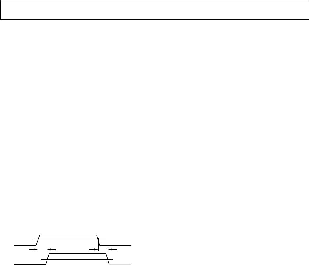
PROPAGATION DELAY-RELATED PARAMETERS
Propagation delay is a parameter that describes the time it takes
a logic signal to propagate through a component. The input-to-
output propagation delay time for a high-to-low transition may
differ from the propagation delay time for a low-to-high
transition.
INPUT (V
Ix
)
OUTPUT (V
Ox
)
t
PLH
t
PHL
50%
50%
10240-013
Figure 13. Propagation Delay Parameters
Pulse width distortion is the maximum difference between
these two propagation delay values and is an indication of how
accurately the timing of the input signal is preserved.
Channel-to-channel matching refers to the maximum amount
that the propagation delay differs between channels within a
single ADuM7240/ADuM7241 component.
Propagation delay skew refers to the maximum amount the
propagation delay differs between multiple ADuM7240/
ADuM7241 components operating under the same conditions.
DC CORRECTNESS
Positive and negative logic transitions at the isolator input cause
narrow (~1 ns) pulses to be sent to the decoder via the transformer.
The decoder is bistable and is, therefore, either set or reset by
the pulses, indicating input logic transitions. In the absence of
logic transitions at the input for more than ~1 µs, a periodic set
of refresh pulses indicative of the correct input state is sent to
ensure dc correctness at the output. If the decoder receives no
internal pulses for more than approximately 5 µs, the input side
is assumed to be unpowered or nonfunctional, and the isolator
output is forced to a default high state by the watchdog timer
circuit.
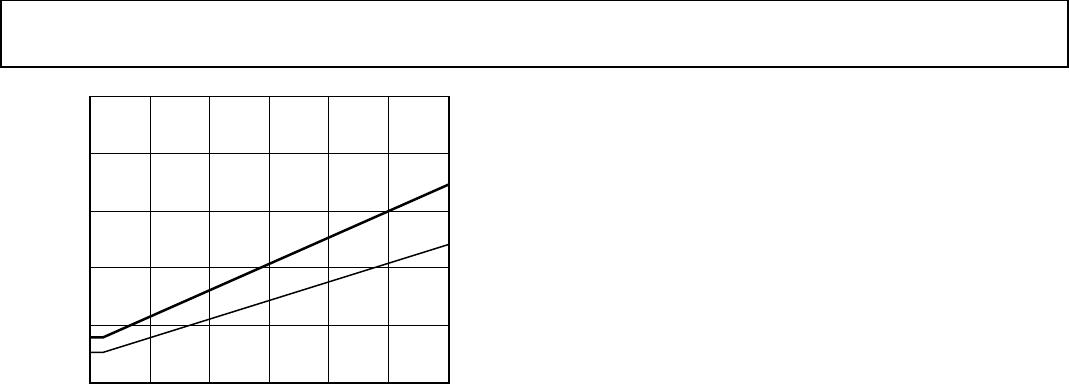
MAGNETIC FIELD IMMUNITY
The magnetic field immunity of the ADuM7240/ADuM7241 is
determined by the changing magnetic field, which induces a
voltage in the transformer’s receiving coil large enough to either
falsely set or reset the decoder. The following analysis defines
the conditions under which this can occur. The 3 V operating
condition of the ADuM7240/ADuM7241 is examined because
it represents the most susceptible mode of operation.
The pulses at the transformer output have an amplitude greater
than 1.0 V. The decoder has a sensing threshold at about 0.5 V, thus
establishing a 0.5 V margin in which induced voltages can be
tolerated. The voltage induced across the receiving coil is given by
V = (−dβ/dt) ∑ π r
n
2
; n = 1, 2, … , N
where:
β is the magnetic flux density (gauss).
r
n
is the radius of the n
th
turn in the receiving coil (cm).
N is the number of turns in the receiving coil.
Given the geometry of the receiving coil in the ADuM7240/
ADuM7241 and an imposed requirement that the induced
voltage be, at most, 50% of the 0.5 V margin at the decoder, a
maximum allowable magnetic field at a given frequency can be
calculated. The result is shown in Figure 14.