Data Sheet ADuM7240/ADuM7241
Rev. B | Page 13 of 16
1000
100
10
1
0.1
0.01
0.001
1k
100M10k
MAXIMUM ALLOWABLE MAGNETIC FLUX (kgauss)
100k 1M
10M
MAGNETIC FIELD FREQUENCY (Hz)
10240-014
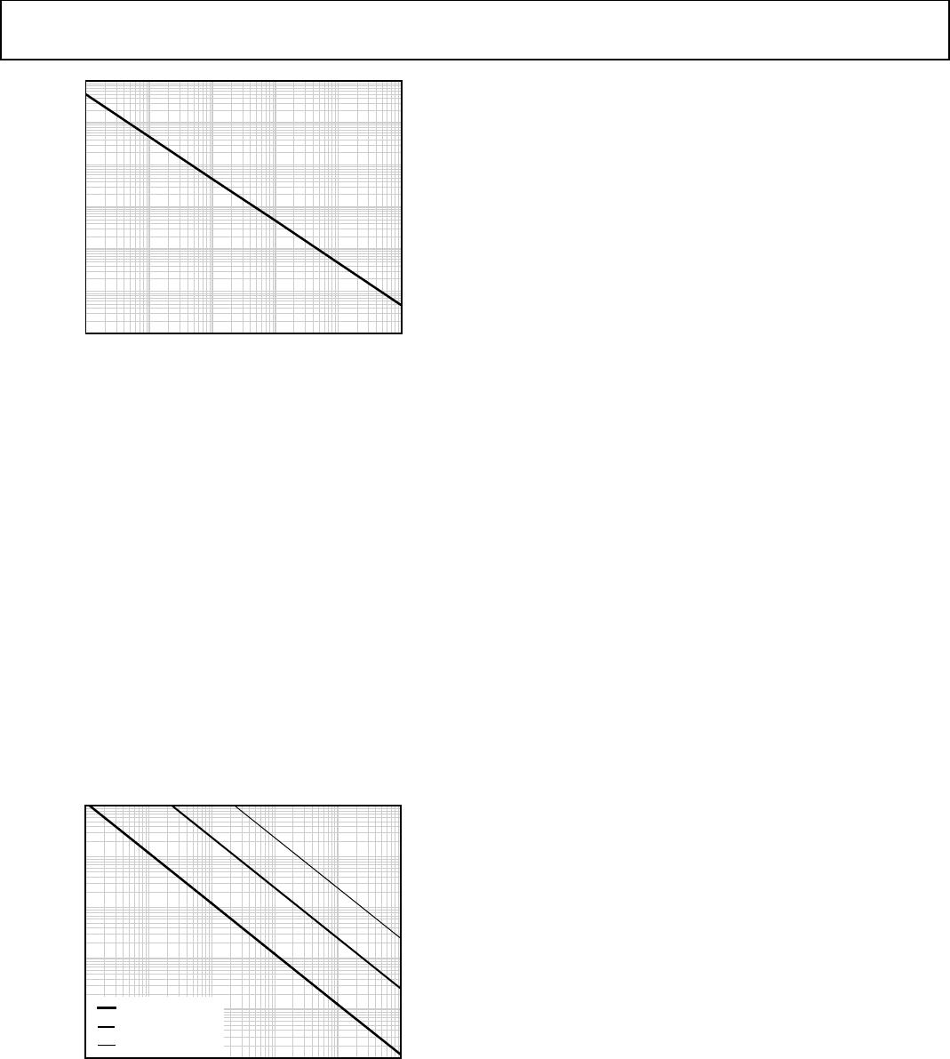
Figure 14. Maximum Allowable External Magnetic Flux Density
For example, at a magnetic field frequency of 1 MHz, the
maximum allowable magnetic field of 0.5 kgauss induces a voltage
of 0.25 V at the receiving coil. This voltage is about 50% of the
sensing threshold and does not cause a faulty output transition.
Similarly, if such an event occurs during a transmitted pulse (and
is of the worst-case polarity), it reduces the received pulse from
>1.0 V to 0.75 V, still well above the 0.5 V sensing threshold of
the decoder.
The preceding magnetic flux density values correspond to
specific current magnitudes at given distances from the
ADuM7240/ADuM7241 transformers. Figure 15 shows these
allowable current magnitudes as a function of frequency for
selected distances. As shown in Figure 15, the ADuM7240/
ADuM7241 is extremely immune and can be affected only by
extremely large currents operated at high frequency very close
to the component. For the 1 MHz example, a 1.2 kA current
placed 5 mm away from the ADuM7240/ADuM7241 is
required to affect the operation of the component.
1000
100
10
1
0.1
0.01
1k
100M10k
MAXIMUM ALLOWABLE CURRENT (kA)
100k 1M
10M
MAGNETIC FIELD FREQUENCY (Hz)
DISTANCE = 5mm
DISTANCE = 100mm
DISTANCE = 1m
10240-015
Figure 15. Maximum Allowable Current for Various
Current-to-ADuM7240/ADuM7241 Spacings
Note that with extreme combinations of strong magnetic field
and high frequency current, loops formed by printed circuit
board traces can induce error voltages large enough to trigger
the thresholds of receiver circuitry. Take care in the layout of
such traces to avoid this possibility.
POWER CONSUMPTION
The supply current at a given channel of the ADuM7240/
ADuM7241 isolator is a function of the supply voltage, the
data rate of the channel, and the output load of the channel.
For each input channel, the supply current is given by
I
DDI
= I
DDI(Q)
f ≤ 0.5 f
r
I
DDI
= I
DDI(D)
× (2f − f
r
) + I
DDI(Q)
f > 0.5 f
r
For each output channel, the supply current is given by
I
DDO
= I
DDO(Q)
f ≤ 0.5 f
r
I
DDO
= (I
DDO(D)
+ (0.5 × 10
−3
) × C
L
× V
DDO
) × (2f − f
r
) + I
DDO(Q)
f > 0.5 f
r
where:
I
DDI(D)
, I
DDO(D)
are the input and output dynamic supply currents
per channel (mA/Mbps).
C
L
is the output load capacitance (pF).
V
DDO
is the output supply voltage (V).
f is the input logic signal frequency (MHz); it is half the input
data rate, expressed in units of Mbps.
f
r
is the input stage refresh rate (Mbps).
I
DDI(Q)
, I
DDO(Q)
are the specified input and output quiescent
supply currents (mA).
To calculate the total V
DD1
and V
DD2
supply current, the supply
currents for each input and output channel corresponding to
V
DD1
and V
DD2
are calculated and totaled. Figure 6 and Figure 7
show per-channel supply currents as a function of data rate for
an unloaded output condition. Figure 8 shows the per-channel
supply current as a function of data rate for a 15 pF output
condition. Figure 9 through Figure 12 show the total V
DD1
and
V
DD2
supply current as a function of data rate for ADuM7240
and ADuM7241 channel configurations.
INSULATION LIFETIME
All insulation structures eventually break down when subjected to
voltage stress over a sufficiently long period. The rate of insulation
degradation is dependent on the characteristics of the voltage
waveform applied across the insulation. In addition to the
testing performed by the regulatory agencies, Analog Devices
carries out an extensive set of evaluations to determine the
lifetime of the insulation structure within the ADuM7240/
ADuM7241.
Analog Devices performs accelerated life testing using voltage levels
higher than the rated continuous working voltage. Acceleration
factors for several operating conditions are determined. These
factors allow calculation of the time to failure at the actual working
voltage. The values shown in Table 18 summarize the working
voltage for 50 years of service life.