LT3480
1
3480fe
For more information www.linear.com/LT3480
TYPICAL APPLICATION
FEATURES
APPLICATIONS
DESCRIPTION
36V, 2A, 2.4MHz Step-Down
Switching Regulator with
70µA Quiescent Current
The LT
®
3480 is an adjustable frequency (200kHz to
2.4MHz) monolithic buck switching regulator that ac-
cepts input voltages up to 36V (60V maximum). A high
efficiency 0.25
switch is included on the die along with
a boost Schottky diode and the necessary oscillator, con-
trol, and logic circuitry. Current mode topology is used
for fast transient response and good loop stability. Low
ripple Burst Mode operation maintains high efficiency at
low output currents while keeping output ripple below
15mV in a typical application. In addition, the LT3480 can
further enhance low output current efficiency by draw-
ing bias current from the output when V
OUT
is above 3V.
Shutdown reduces input supply current to less than 1µA
while a resistor and capacitor on the RUN/SS pin provide a
controlled output voltage ramp (soft-start). A power good
flag signals when V
OUT
reaches 86% of the programmed
output voltage. The LT3480 is available in 10-lead MSOP
and 3mm × 3mm DFN packages with exposed pads for
low thermal resistance.
n
Wide Input Range:
Operation from 3.6V to 36V
Over-Voltage Lockout Protects Circuits
through 60V Transients
n
2A Maximum Output Current
n
Low Ripple Burst Mode
®
Operation
70µA I
Q
at 12V
IN
to 3.3V
OUT
Output Ripple < 15mV
n
Adjustable Switching Frequency: 200kHz to 2.4MHz
n
Low Shutdown Current: I
Q
< 1µA
n
Integrated Boost Diode
n
Synchronizable Between 250kHz to 2MHz
n
Power Good Flag
n
Saturating Switch Design: 0.25 On-Resistance
n
0.790V Feedback Reference Voltage
n
Output Voltage: 0.79V to 20V
n
Soft-Start Capability
n
Small 10-Lead Thermally Enhanced MSOP and
(3mm × 3mm) DFN Packages
n
Automotive Battery Regulation
n
Power for Portable Products
n
Distributed Supply Regulation
n
Industrial Supplies
, LT, LTC and LTM are registered trademarks of Linear Technology Corporation.
Burst Mode is a registered trademark of Linear Technology Corporation. All other
trademarks are the property of their respective owners.
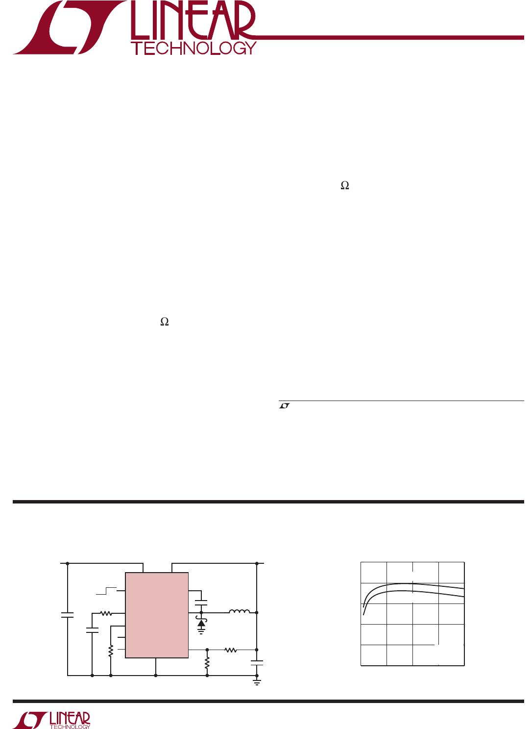
3.3V Step-Down Converter
SW
FB
V
C
PG
RT
V
IN
BD
V
IN
4.5V TO 36V
TRANSIENT
TO 60V
V
OUT
3.3V
2A
4.7µF
0.47µF
470pF
22µF
100k
14k
40.2k
4.7µH
316k
GND
OFF ON
LT3480
3480 TA01
RUN/SS BOOST
SYNC
Efficiency
LOAD CURRENT (A)
0
EFFICIENCY (%)
50
0.5 1.0 1.5 2
3480 TA01b
60
100
90
80
70
V
IN
= 12V
L = 5.6µH
F = 800 kHz
V
OUT
= 3.3V
V
OUT
= 5V
LT3480
2
3480fe
For more information www.linear.com/LT3480
ABSOLUTE MAXIMUM RATINGS
V
IN
, RUN/SS Voltage (Note 5) ...................................60V
BOOST Pin Voltage
...................................................56V
BOOST Pin Above SW Pin
.........................................30V
FB, RT, V
C
Voltage .......................................................5V
PG, BD, SYNC Voltage
..............................................30V
Operating Junction Temperature Range (Note 2)
LT3480E
............................................. –40°C to 125°C
LT3480I
.............................................. –40°C to 125°C
LT3480H ............................................ –40°C to 150°C
LT3480MP.......................................... –55°C to 150°C
(Note 1)
TOP VIEW
DD PACKAGE
10-LEAD (3mm × 3mm) PLASTIC DFN
10
9
6
7
8
4
5
3
11
2
1
RT
V
C
FB
PG
SYNC
BD
BOOST
SW
V
IN
RUN/SS
JA
= 45°C/W,
JC
= 10°C/W
EXPOSED PAD (PIN 11) IS GND, MUST BE SOLDERED TO PCB
1
2
3
4
5
BD
BOOST
SW
V
IN
RUN/SS
10
9
8
7
6
RT
V
C
FB
PG
SYNC
TOP VIEW
MSE PACKAGE
10-LEAD PLASTIC MSOP
11
JA
= 45°C/W,
JC
= 10°C/W
EXPOSED PAD (PIN 11) IS GND, MUST BE SOLDERED TO PCB
PIN CONFIGURATION
ORDER INFORMATION
LEAD FREE FINISH TAPE AND REEL PART MARKING* PACKAGE DESCRIPTION TEMPERATURE RANGE
LT3480EDD#PBF LT3480EDD#TRPBF LCTP
10-Lead (3mm × 3mm) Plastic DFN
–40°C to 125°C
LT3480IDD#PBF LT3480IDD#TRPBF LCTP
10-Lead (3mm × 3mm) Plastic DFN
–40°C to 125°C
LT3480EMSE#PBF LT3480EMSE#TRPBF LTCTM 10-Lead Plastic MSOP –40°C to 125°C
LT3480IMSE#PBF LT3480IMSE#TRPBF LTCTM 10-Lead Plastic MSOP –40°C to 125°C
LT3480HMSE#PBF LT3480HMSE#TRPBF LTCTM 10-Lead Plastic MSOP –40°C to 150°C
LT3480MPMSE#PBF LT3480MPMSE#TRPBF LTCTM 10-Lead Plastic MSOP –55°C to 150°C
LEAD BASED FINISH TAPE AND REEL PART MARKING* PACKAGE DESCRIPTION TEMPERATURE RANGE
LT3480EDD LT3480EDD#TR LCTP
10-Lead (3mm × 3mm) Plastic DFN
–40°C to 125°C
LT3480IDD LT3480IDD#TR LCTP
10-Lead (3mm × 3mm) Plastic DFN
–40°C to 125°C
LT3480EMSE LT3480EMSE#TR LTCTM 10-Lead Plastic MSOP –40°C to 125°C
LT3480IMSE LT3480IMSE#TR LTCTM 10-Lead Plastic MSOP –40°C to 125°C
LT3480HMSE LT3480HMSE#TR LTCTM 10-Lead Plastic MSOP –40°C to 150°C
LT3480MPMSE LT3480MPMSE#TR LTCTM 10-Lead Plastic MSOP –55°C to 150°C
Consult LTC Marketing for parts specified with wider operating temperature ranges. *The temperature grade is identified by a label on the shipping container.
For more information on lead free part marking, go to: http://www.linear.com/leadfree/
For more information on tape and reel specifications, go to: http://www.linear.com/tapeandreel/
Storage Temperature Range ................... –65°C to 150°C
Lead Temperature (Soldering, 10 sec)
(MSE Only)
....................................................... 300°C
LT3480
3
3480fe
For more information www.linear.com/LT3480
Note 1: Stresses beyond those listed under Absolute Maximum Ratings
may cause permanent damage to the device. Exposure to any Absolute
Maximum Rating condition for extended periods may affect device
reliability and lifetime.
The l denotes the specifications which apply over the full operating temperature
range, otherwise specifications are at T
A
= 25°C. V
IN
= 10V, V
RUN/SS
= 10V, V
BOOST
= 15V, V
BD
= 3.3V unless otherwise noted. (Note 2)
Note 2: The LT3480E is guaranteed to meet performance specifications
from 0°C to 125°C. Specifications over the –40°C to 125°C operating
temperature range are assured by design, characterization and correlation
with statistical process controls. The LT3480I specifications are
PARAMETER CONDITIONS MIN TYP MAX UNITS
Minimum Input Voltage
l
3 3.6 V
V
IN
Overvoltage Lockout
l
36 38 40 V
Quiescent Current from V
IN
V
RUN/SS
= 0.2V
V
BD
= 3V, Not Switching
V
BD
= 0, Not Switching
l
0.01
30
105
0.5
100
160
µA
µA
µA
Quiescent Current from BD V
RUN/SS
= 0.2V
V
BD
= 3V, Not Switching
V
BD
= 0, Not Switching
l
0.01
80
1
0.5
120
5
µA
µA
µA
Minimum Bias Voltage (BD Pin) 2.7 3 V
Feedback Voltage
l
780
775
790
790
800
805
mV
mV
FB Pin Bias Current (Note 3) V
FB
= 0.8V, V
C
= 0.4V
l
7 30 nA
FB Voltage Line Regulation 4V < V
IN
< 36V 0.002 0.01 %/V
Error Amp g
m
400 µMho
Error Amp Gain 1000
V
C
Source Current 45 µA
V
C
Sink Current 45 µA
V
C
Pin to Switch Current Gain 3.5 A/V
V
C
Clamp Voltage 2 V
Switching Frequency R
T
= 8.66k
R
T
= 29.4k
R
T
= 187k
2.1
0.9
160
2.4
1
200
2.7
1.15
240
MHz
MHz
kHz
Minimum Switch Off-Time
l
60 150 nS
Switch Current Limit Duty Cycle = 5% 3 3.5 4 A
Switch V
CESAT
I
SW
= 2A 500 mV
Boost Schottky Reverse Leakage V
BD
= 0V 0.02 2 µA
Minimum Boost Voltage (Note 4)
l
1.5 2.1 V
BOOST Pin Current I
SW
= 1A 22 35 mA
RUN/SS Pin Current V
RUN/SS
= 2.5V 5 10 µA
RUN/SS Input Voltage High 2.5 V
RUN/SS Input Voltage Low 0.2 V
PG Threshold Offset from Feedback Voltage V
FB
Rising 100 mV
PG Hysteresis 12 mV
PG Leakage V
PG
= 5V 0.1 1 µA
PG Sink Current V
PG
= 0.4V
l
100 600 µA
SYNC Low Threshold 0.5 V
SYNC High Threshold 0.7 V
SYNC Pin Bias Current V
SYNC
= 0V 0.1 µA
ELECTRICAL CHARACTERISTICS

LT3480IDD#PBF

Mfr. #:
Manufacturer:
Analog Devices / Linear Technology
Description:
Switching Voltage Regulators 38V, 2A, 2.4MHz Step-Down Switching Reg in DFN
Lifecycle:
New from this manufacturer.
Delivery:
DHL FedEx Ups TNT EMS
Payment:
T/T Paypal Visa MoneyGram Western Union