LT3480
7
3480fe
For more information www.linear.com/LT3480
PIN FUNCTIONS
BD (Pin 1): This pin connects to the anode of the boost
Schottky diode. BD also supplies current to the internal
regulator. BD must be locally bypassed when not tied to
V
OUT
with a low ESR capacitor (1µF).
BOOST (Pin 2): This pin is used to provide a drive
voltage, higher than the input voltage, to the internal bipolar
NPN power switch.
SW (Pin 3): The SW pin is the output of the internal power
switch. Connect this pin to the inductor, catch diode and
boost capacitor.
V
IN
(Pin 4): The V
IN
pin supplies current to the LT3480’s
internal regulator and to the internal power switch. This
pin must be locally bypassed.
RUN/SS (Pin 5): The RUN/SS pin is used to put the
LT3480 in shutdown mode. Tie to ground to shut down
the LT3480. Tie to 2.5V or more for normal operation. If
the shutdown feature is not used, tie this pin to the V
IN
pin. RUN/SS also provides a soft-start function; see the
Applications Information section.
SYNC (Pin 6): This is the external clock synchronization
input. Ground this pin for low ripple Burst Mode operation at
low output loads. Tie to a clock source for synchronization.
Clock edges should have rise and fall times faster than 1µs.
See synchronizing section in Applications Information.
PG (Pin 7): The PG pin is the open collector output of an
internal comparator. PG remains low until the FB pin is
within 14% of the final regulation voltage. PG output is
valid when V
IN
is above 3.6V and RUN/SS is high.
FB (Pin 8): The LT3480 regulates the FB pin to 0.790V.
Connect the feedback resistor divider tap to this pin.
V
C
(Pin 9): The V
C
pin is the output of the internal error
amplifier. The voltage on this pin controls the peak switch
current. Tie an RC network from this pin to ground to
compensate the control loop.
RT (Pin 10): Oscillator Resistor Input. Connecting a resistor
to ground from this pin sets the switching frequency.
Exposed Pad (Pin 11): Ground. The exposed pad must
be soldered to PCB.
3480 G25
I
L
0.2A/DIV
V
SW
5V/DIV
V
OUT
10mV/DIV
V
IN
= 12V; FRONT PAGE APPLICATION
I
LOAD
= 110mA
1µs/DIV
3480 G26
I
L
0.5A/DIV
V
SW
5V/DIV
V
OUT
10mV/DIV
V
IN
= 12V; FRONT PAGE APPLICATION
I
LOAD
= 1A
1µs/DIV
Switching Waveforms; Transition
from Burst Mode to Full Frequency
Switching Waveforms; Full
Frequency Continuous Operation
TYPICAL PERFORMANCE CHARACTERISTICS
LT3480
8
3480fe
For more information www.linear.com/LT3480
OPERATION
The LT3480 is a constant frequency, current mode step-
down regulator. An oscillator, with frequency set by RT,
enables an RS flip-flop, turning on the internal power
switch. An amplifier and comparator monitor the current
flowing between the V
IN
and SW pins, turning the switch
off when this current reaches a level determined by the
voltage at V
C
. An error amplifier measures the output
voltage through an external resistor divider tied to the FB
pin and servos the V
C
pin. If the error amplifiers output
increases, more current is delivered to the output; if it
decreases, less current is delivered. An active clamp on the
V
C
pin provides current limit. The V
C
pin is also clamped to
the voltage on the RUN/SS pin; soft-start is implemented
by generating a voltage ramp at the RUN/SS pin using an
external resistor and capacitor.
An internal regulator provides power to the control circuitry.
The bias regulator normally draws power from the V
IN
pin,
but if the BD pin is connected to an external voltage higher
than 3V bias power will be drawn from the external source
(typically the regulated output voltage). This improves
efficiency. The RUN/SS pin is used to place the LT3480
in shutdown, disconnecting the output and reducing the
input current to less than 1µA.
The switch driver operates from either the input or from
the BOOST pin. An external capacitor and diode are used
to generate a voltage at the BOOST pin that is higher than
the input supply. This allows the driver to fully saturate the
internal bipolar NPN power switch for efficient operation.
To further optimize efficiency, the LT3480 automatically
switches to Burst Mode operation in light load situations.
Between bursts, all circuitry associated with controlling
the output switch is shut down, reducing the input supply
current to 70µA in a typical application.
The oscillator reduces the LT3480’s operating frequency when
the voltage at the FB pin is low. This frequency foldback helps
to control the output current during startup and overload.
BLOCK DIAGRAM
+
+
+
OSCILLATOR
200kHz–2.4MHz
Burst Mode
DETECT
V
C
CLAMP
SOFT-START
SLOPE COMP
R
V
IN
V
IN
RUN/SS
BOOST
SW
SWITCH
LATCH
V
C
V
OUT
C2
C3
C
F
L1
D1
DISABLE
C
C
R
C
BD
RT
R2
GND
ERROR AMP
R1
FB
R
T
C1
PG
0.7V
S
Q
Σ
3480 BD
4
5
10
7
1
2
3
9
11 8
6
INTERNAL 0.79V REF
SYNC
LT3480
9
3480fe
For more information www.linear.com/LT3480
APPLICATIONS INFORMATION
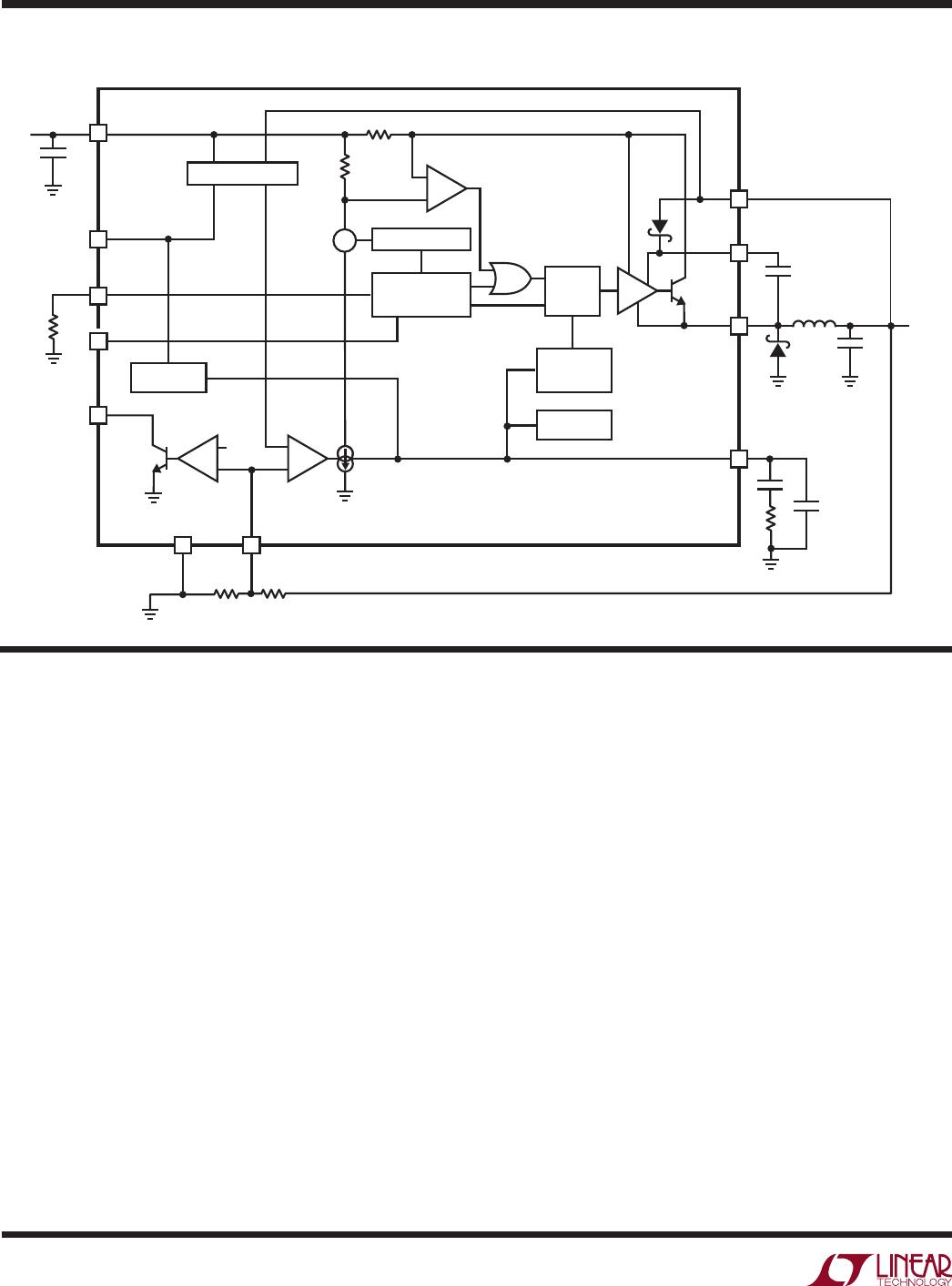
OPERATION
FB Resistor Network
The output voltage is programmed with a resistor divider
between the output and the FB pin. Choose the 1% resis-
tors according to:
R1=R2
V
OUT
0.79V
1
Reference designators refer to the Block Diagram.
Setting the Switching Frequency
The LT3480 uses a constant frequency PWM architecture
that can be programmed to switch from 200kHz to 2.4MHz
by using a resistor tied from the RT pin to ground. A table
showing the necessary R
T
value for a desired switching
frequency is in Figure 1.
SWITCHING FREQUENCY (MHz)
R
T
VALUE (k)
0.2
0.3
0.4
0.5
0.6
0.7
0.8
0.9
1.0
1.2
1.4
1.6
1.8
2.0
2.2
2.4
187
121
88.7
68.1
56.2
46.4
40.2
34
29.4
23.7
19.1
16.2
13.3
11.5
9.76
8.66
Figure 1. Switching Frequency vs. R
T
Value
Operating Frequency Tradeoffs
Selection of the operating frequency is a tradeoff between
efficiency, component size, minimum dropout voltage, and
maximum input voltage. The advantage of high frequency
operation is that smaller inductor and capacitor values may
be used. The disadvantages are lower efficiency, lower
maximum input voltage, and higher dropout voltage. The
highest acceptable switching frequency (f
SW(MAX)
) for a
given application can be calculated as follows:
f
SW(MAX)
=
V
D
+ V
OUT
t
ON(MIN)
V
D
+ V
IN
V
SW
(
)
where V
IN
is the typical input voltage, V
OUT
is the output
voltage, V
D
is the catch diode drop (~0.5V) and V
SW
is the
internal switch drop (~0.5V at max load). This equation
shows that slower switching frequency is necessary to
safely accommodate high V
IN
/V
OUT
ratio. Also, as shown
in the next section, lower frequency allows a lower dropout
voltage. The reason input voltage range depends on the
switching frequency is because the LT3480 switch has finite
minimum on and off times. The switch can turn on for a
minimum of ~150ns and turn off for a minimum of ~150ns.
Typical minimum on time at 25°C is 80ns. This means that
the minimum and maximum duty cycles are:
DC
MIN
= f
SW
t
ON(MIN)
DC
MAX
= 1 f
SW
t
OFF(MIN
)
where f
SW
is the switching frequency, the t
ON(MIN)
is the
minimum switch on time (~150ns), and the t
OFF(MIN)
is
the minimum switch off time (~150ns). These equations
show that duty cycle range increases when switching
frequency is decreased.
The LT3480 contains a power good comparator which trips
when the FB pin is at 86% of its regulated value. The PG
output is an open-collector transistor that is off when the
output is in regulation, allowing an external resistor to pull
the PG pin high. Power good is valid when the LT3480 is
enabled and V
IN
is above 3.6V.
The LT3480 has an overvoltage protection feature which
disables switching action when the V
IN
goes above 38V
typical (36V minimum). When switching is disabled, the
LT3480 can safely sustain input voltages up to 60V.

LT3480IDD#PBF

Mfr. #:
Manufacturer:
Analog Devices / Linear Technology
Description:
Switching Voltage Regulators 38V, 2A, 2.4MHz Step-Down Switching Reg in DFN
Lifecycle:
New from this manufacturer.
Delivery:
DHL FedEx Ups TNT EMS
Payment:
T/T Paypal Visa MoneyGram Western Union