LT3480
10
3480fe
For more information www.linear.com/LT3480
APPLICATIONS INFORMATION
A good choice of switching frequency should allow ad-
equate input voltage range (see next section) and keep
the inductor and capacitor values small.
Input Voltage Range
The maximum input voltage for LT3480 applications depends
on switching frequency, the Absolute Maximum Ratings of
the V
IN
and BOOST pins, and the operating mode.
The LT3480 can operate from input voltages up to 38V,
and safely withstand input voltages up 60V. Note that while
V
IN
>38V (typical), the LT3480 will stop switching, allowing
the output to fall out of regulation.
While the output is in start-up, short-circuit, or other
overload conditions, the switching frequency should be
chosen according to the following discussion.
For safe operation at inputs up to 60V the switching fre-
quency must be set low enough to satisfy V
IN(MAX)
≥ 40V
according to the following equation. If lower V
IN(MAX)
is
desired, this equation can be used directly.
V
IN(MAX)
=
V
OUT
+ V
D
f
SW
t
ON(MIN)
V
D
+ V
SW
where V
IN(MAX)
is the maximum operating input voltage,
V
OUT
is the output voltage, V
D
is the catch diode drop
(~0.5V), V
SW
is the internal switch drop (~0.5V at max
load), f
SW
is the switching frequency (set by R
T
), and
t
ON(MIN)
is the minimum switch on time (~150ns). Note that
a higher switching frequency will depress the maximum
operating input voltage. Conversely, a lower switching
frequency will be necessary to achieve safe operation at
high input voltages.
If the output is in regulation and no short-circuit, start-
up, or overload events are expected, then input voltage
transients of up to 60V are acceptable regardless of the
switching frequency. In this mode, the LT3480 may enter
pulse skipping operation where some switching pulses
are skipped to maintain output regulation. In this mode
the output voltage ripple and inductor current ripple will
be higher than in normal operation. Above 38V switching
will stop.
The minimum input voltage is determined by either the
LT3480’s minimum operating voltage of ~3.6V or by its
maximum duty cycle (see equation in previous section).
The minimum input voltage due to duty cycle is:
V
IN(MIN)
=
V
OUT
+ V
D
1 f
SW
t
OFF(MIN)
V
D
+ V
SW
where V
IN(MIN)
is the minimum input voltage, and t
OFF(MIN)
is the minimum switch off time (150ns). Note that higher
switching frequency will increase the minimum input
voltage. If a lower dropout voltage is desired, a lower
switching frequency should be used.
Inductor Selection
For a given input and output voltage, the inductor value
and switching frequency will determine the ripple current.
The ripple current ΔI
L
increases with higher V
IN
or V
OUT
and decreases with higher inductance and faster switching
frequency. A reasonable starting point for selecting the
ripple current is:
ΔI
L
= 0.4(I
OUT(MAX)
)
where I
OUT(MAX)
is the maximum output load current. To
guarantee sufficient output current, peak inductor current
must be lower than the LT3480’s switch current limit (I
LIM
).
The peak inductor current is:
I
L(PEAK)
= I
OUT(MAX)
+ ΔI
L
/2
where I
L(PEAK)
is the peak inductor current, I
OUT(MAX)
is
the maximum output load current, and ΔI
L
is the inductor
ripple current. The LT3480’s switch current limit (I
LIM
) is
at least 3.5A at low duty cycles and decreases linearly to
2.5A at DC = 0.8. The maximum output current is a func-
tion of the inductor ripple current:
I
OUT(MAX)
= I
LIM
ΔI
L
/2
Be sure to pick an inductor ripple current that provides
sufficient maximum output current (I
OUT(MAX)
).
The largest inductor ripple current occurs at the highest
V
IN
. To guarantee that the ripple current stays below the
specified maximum, the inductor value should be chosen
according to the following equation:
L =
V
OUT
+ V
D
f
SW
I
L
1
V
OUT
+ V
D
V
IN(MAX)
LT3480
11
3480fe
For more information www.linear.com/LT3480
APPLICATIONS INFORMATION
where V
D
is the voltage drop of the catch diode (~0.4V),
V
IN(MAX)
is the maximum input voltage, V
OUT
is the output
voltage, f
SW
is the switching frequency (set by RT), and L
is in the inductor value.
The inductors RMS current rating must be greater than the
maximum load current and its saturation current should be
about 30% higher. For robust operation in fault conditions
(start-up or short circuit) and high input voltage (>30V),
the saturation current should be above 3.5A. To keep the
efficiency high, the series resistance (DCR) should be less
than 0.1
, and the core material should be intended for
high frequency applications. Table 1 lists several vendors
and suitable types.
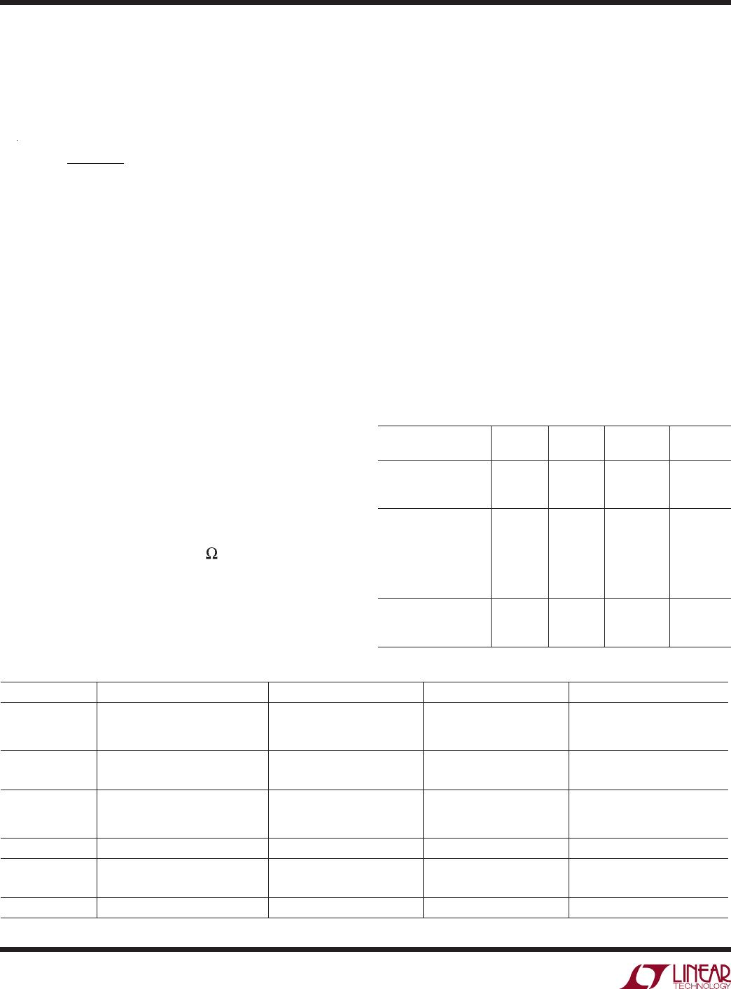
Table 1. Inductor Vendors
VENDOR URL PART SERIES TYPE
Murata www.murata.com LQH55D Open
TDK www.componenttdk.com SLF7045
SLF10145
Shielded
Shielded
Toko www.toko.com D62CB
D63CB
D75C
D75F
Shielded
Shielded
Shielded
Open
Sumida www.sumida.com CR54
CDRH74
CDRH6D38
CR75
Open
Shielded
Shielded
Open
Of course, such a simple design guide will not always re-
sult in the optimum inductor for your application. A larger
value inductor provides a slightly higher maximum load
current and will reduce the output voltage ripple. If your
load is lower than 2A, then you can decrease the value of
the inductor and operate with higher ripple current. This
allows you to use a physically smaller inductor, or one
with a lower DCR resulting in higher efficiency. There are
several graphs in the Typical Performance Characteristics
section of this data sheet that show the maximum load
current as a function of input voltage and inductor value
for several popular output voltages. Low inductance may
result in discontinuous mode operation, which is okay
but further reduces maximum load current. For details of
maximum output current and discontinuous mode opera-
tion, see Linear Technology Application Note 44. Finally,
for duty cycles greater than 50% (V
OUT
/V
IN
> 0.5), there
is a minimum inductance required to avoid subharmonic
oscillations. See AN19.
Input Capacitor
Bypass the input of the LT3480 circuit with a ceramic capaci-
tor of X7R or X5R type. Y5V types have poor performance
over temperature and applied voltage, and should not be
used. A 4.7µF to 10µF ceramic capacitor is adequate to
bypass the LT3480 and will easily handle the ripple current.
Note that larger input capacitance is required when a lower
switching frequency is used. If the input power source has
high impedance, or there is significant inductance due to
long wires or cables, additional bulk capacitance may be
necessary. This can be provided with a lower performance
electrolytic capacitor.
Step-down regulators draw current from the input sup-
ply in pulses with very fast rise and fall times. The input
capacitor is required to reduce the resulting voltage
ripple at the LT3480 and to force this very high frequency
switching current into a tight local loop, minimizing EMI.
A 4.7µF capacitor is capable of this task, but only if it is
placed close to the LT3480 and the catch diode (see the
PCB Layout section). A second precaution regarding the
ceramic input capacitor concerns the maximum input
voltage rating of the LT3480. A ceramic input capacitor
combined with trace or cable inductance forms a high
quality (under damped) tank circuit. If the LT3480 circuit
is plugged into a live supply, the input voltage can ring to
twice its nominal value, possibly exceeding the LT3480’s
voltage rating. This situation is easily avoided (see the Hot
Plugging Safely section).
For space sensitive applications, a 2.2µF ceramic capaci-
tor can be used for local bypassing of the LT3480 input.
However, the lower input capacitance will result in in-
creased input current ripple and input voltage ripple, and
may couple noise into other circuitry. Also, the increased
voltage ripple will raise the minimum operating voltage
of the LT3480 to ~3.7V.
Output Capacitor and Output Ripple
The output capacitor has two essential functions. Along
with the inductor, it filters the square wave generated by the
LT3480 to produce the DC output. In this role it determines
the output ripple, and low impedance at the switching
frequency is important. The second function is to store
LT3480
12
3480fe
For more information www.linear.com/LT3480
APPLICATIONS INFORMATION
Table 2. Capacitor Vendors
VENDOR PHONE URL PART SERIES COMMANDS
Panasonic (714) 373-7366 www.panasonic.com Ceramic,
Polymer,
Tantalum
EEF Series
Kemet (864) 963-6300 www.kemet.com Ceramic,
Tantalum
T494, T495
Sanyo (408) 749-9714 www.sanyovideo.com Ceramic,
Polymer,
Tantalum
POSCAP
Murata (408) 436-1300 www.murata.com Ceramic
AVX www.avxcorp.com Ceramic,
Tantalum
TPS Series
Taiyo Yuden (864) 963-6300 www.taiyo-yuden.com Ceramic
energy in order to satisfy transient loads and stabilize the
LT3480’s control loop. Ceramic capacitors have very low
equivalent series resistance (ESR) and provide the best
ripple performance. A good starting value is:
C
OUT
=
100
V
OUT
f
SW
where f
SW
is in MHz, and C
OUT
is the recommended output
capacitance in µF. Use X5R or X7R types. This choice will
provide low output ripple and good transient response.
Transient performance can be improved with a higher value
capacitor if the compensation network is also adjusted
to maintain the loop bandwidth. A lower value of output
capacitor can be used to save space and cost but transient
performance will suffer. See the Frequency Compensation
section to choose an appropriate compensation network.
When choosing a capacitor, look carefully through the
data sheet to find out what the actual capacitance is under
operating conditions (applied voltage and temperature).
A physically larger capacitor, or one with a higher voltage
rating, may be required. High performance tantalum or
electrolytic capacitors can be used for the output capacitor.
Low ESR is important, so choose one that is intended for
use in switching regulators. The ESR should be specified
by the supplier, and should be 0.05
or less. Such a capaci-
tor will be larger than a ceramic capacitor and will have a
larger capacitance, because the capacitor must be large to
achieve low ESR. Table 2 lists several capacitor vendors.
Catch Diode
The catch diode conducts current only during switch off
time. Average forward current in normal operation can
be calculated from:
I
D(AVG)
= I
OUT
(V
IN
– V
OUT
)/V
IN
where I
OUT
is the output load current. The only reason to
consider a diode with a larger current rating than necessary
for nominal operation is for the worst-case condition of
shorted output. The diode current will then increase to the
typical peak switch current. Peak reverse voltage is equal
to the regulator input voltage. Use a Schottky diode with a
reverse voltage rating greater than the input voltage. The
overvoltage protection feature in the LT3480 will keep the
switch off when V
IN
> 38V which allows the use of 40V
rated Schottky even when V
IN
ranges up to 60V. Table 3
lists several Schottky diodes and their manufacturers.
Table 3. Diode Vendors
PART NUMBER
V
R
(V)
I
AVE
(A)
V
F
AT 1A
(mV)
V
F
AT 2A
(mV)
On Semiconductor
MBRM120E
MBRM140
20
40
1
1
530
550
595
Diodes Inc.
B120
B130
B220
B230
DFLS240L
20
30
20
30
40
1
1
2
2
2
500
500
500
500
500
International Rectifier
10BQ030
20BQ030
30
30
1
2
420
470
470

LT3480IDD#PBF

Mfr. #:
Manufacturer:
Analog Devices / Linear Technology
Description:
Switching Voltage Regulators 38V, 2A, 2.4MHz Step-Down Switching Reg in DFN
Lifecycle:
New from this manufacturer.
Delivery:
DHL FedEx Ups TNT EMS
Payment:
T/T Paypal Visa MoneyGram Western Union