LT3480
13
3480fe
For more information www.linear.com/LT3480
APPLICATIONS INFORMATION
+
0.8V
SW
V
C
g
m
=
420µmho
GND
3M
LT3480
3480 F02
R1
OUTPUT
ESR
C
F
C
C
R
C
ERROR
AMPLIFIER
FB
R2
C1
C1
CURRENT MODE
POWER STAGE
g
m
= 3.5mho
+
POLYMER
OR
TANTALUM
CERAMIC
C
PL
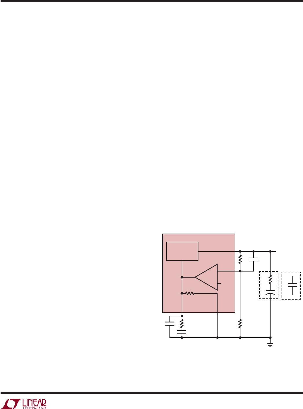
Figure 2. Model for Loop Response
Ceramic Capacitors
Ceramic capacitors are small, robust and have very low
ESR. However, ceramic capacitors can cause problems
when used with the LT3480 due to their piezoelectric nature.
When in Burst Mode operation, the LT3480’s switching
frequency depends on the load current, and at very light
loads the LT3480 can excite the ceramic capacitor at audio
frequencies, generating audible noise. Since the LT3480
operates at a lower current limit during Burst Mode
operation, the noise is typically very quiet to a casual ear.
If this is unacceptable, use a high performance tantalum
or electrolytic capacitor at the output.
A final precaution regarding ceramic capacitors concerns
the maximum input voltage rating of the LT3480. A ceramic
input capacitor combined with trace or cable inductance
forms a high quality (under damped) tank circuit. If the
LT3480 circuit is plugged into a live supply, the input volt-
age can ring to twice its nominal value, possibly exceeding
the LT3480’s rating. This situation is easily avoided (see
the Hot Plugging Safely section).
Frequency Compensation
The LT3480 uses current mode control to regulate the
output. This simplifies loop compensation. In particular, the
LT3480 does not require the ESR of the output capacitor
for stability, so you are free to use ceramic capacitors to
achieve low output ripple and small circuit size. Frequency
compensation is provided by the components tied to the
V
C
pin, as shown in Figure 2. Generally a capacitor (C
C
)
and a resistor (R
C
) in series to ground are used. In addi-
tion, there may be lower value capacitor in parallel. This
capacitor (C
F
) is not part of the loop compensation but
is used to filter noise at the switching frequency, and is
required only if a phase-lead capacitor is used or if the
output capacitor has high ESR.
Loop compensation determines the stability and transient
performance. Designing the compensation network is
a bit complicated and the best values depend on the
application and in particular the type of output capacitor.
A practical approach is to start with one of the circuits in
this data sheet that is similar to your application and tune
the compensation network to optimize the performance.
Stability should then be checked across all operating
conditions, including load current, input voltage and
temperature. The LT1375 data sheet contains a more
thorough discussion of loop compensation and describes
how to test the stability using a transient load. Figure 2
shows an equivalent circuit for the LT3480 control loop.
The error amplifier is a transconductance amplifier with
finite output impedance. The power section, consisting
of the modulator, power switch and inductor, is modeled
as a transconductance amplifier generating an output
current proportional to the voltage at the V
C
pin. Note that
the output capacitor integrates this current, and that the
capacitor on the V
C
pin (C
C
) integrates the error amplifier
output current, resulting in two poles in the loop. In most
cases a zero is required and comes from either the output
capacitor ESR or from a resistor R
C
in series with C
C
.
This simple model works well as long as the value of the
inductor is not too high and the loop crossover frequency
is much lower than the switching frequency. A phase lead
capacitor (C
PL
) across the feedback divider may improve
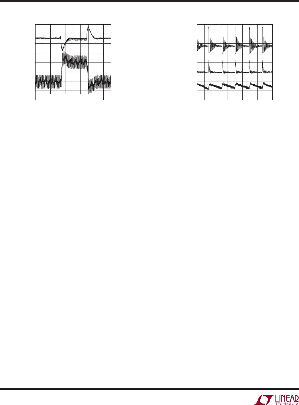
the transient response. Figure 3 shows the transient
response when the load current is stepped from 500mA
to 1500mA and back to 500mA.
LT3480
14
3480fe
For more information www.linear.com/LT3480
APPLICATIONS INFORMATION
Figure 4. Burst Mode Operation
3480 F04
I
L
0.2A/DIV
V
SW
5V/DIV
V
OUT
10mV/DIV
5µs/DIV
V
IN
= 12V; FRONT PAGE APPLICATION
I
LOAD
= 10mA
Figure 3. Transient Load Response of the LT3480 Front Page
Application as the Load Current Is Stepped from 500mA to
1500mA. V
OUT
= 3.3V
3480 F03
I
L
0.5A/DIV
V
OUT
100mV/DIV
10µs/DIV
V
IN
= 12V; FRONT PAGE APPLICATION
Low-Ripple Burst Mode and Pulse-Skip Mode
The LT3480 is capable of operating in either Low-Ripple
Burst Mode or Pulse-Skip Mode which are selected using
the SYNC pin. See the Synchronization section for details.
To enhance efficiency at light loads, the LT3480 can be
operated in Low-Ripple Burst Mode operation which keeps
the output capacitor charged to the proper voltage while
minimizing the input quiescent current. During Burst Mode
operation, the LT3480 delivers single cycle bursts of current
to the output capacitor followed by sleep periods where
the output power is delivered to the load by the output
capacitor. Because the LT3480 delivers power to the output
with single, low current pulses, the output ripple is kept
below 15mV for a typical application. In addition, V
IN
and
BD quiescent currents are reduced to typically 30µA and
80µA respectively during the sleep time. As the load cur-
rent decreases towards a no load condition, the percentage
of time that the LT3480 operates in sleep mode increases
and the average input current is greatly reduced resulting
in high efficiency even at very low loads. See Figure 4.
At higher output loads (above 140mA for the front page
application) the LT3480 will be running at the frequency
programmed by the R
T
resistor, and will be operating in
standard PWM mode. The transition between PWM and
Low-Ripple Burst Mode is seamless, and will not disturb
the output voltage.
If low quiescent current is not required the LT3480 can
operate in Pulse-Skip mode. The benefit of this mode is
that the LT3480 will enter full frequency standard PWM
operation at a lower output load current than when in
Burst Mode. The front page application circuit will switch
at full frequency at output loads higher than about 60mA.
BOOST and BIAS Pin Considerations
Capacitor C3 and the internal boost Schottky diode (see
the Block Diagram) are used to generate a boost volt-
age that is higher than the input voltage. In most cases
a 0.22µF capacitor will work well. Figure 2 shows three
ways to arrange the boost circuit. The BOOST pin must be
more than 2.3V above the SW pin for best efficiency. For
outputs of 3V and above, the standard circuit (Figure 5a)
is best. For outputs between 2.8V and 3V, use a 1µF boost
capacitor. A 2.5V output presents a special case because it
is marginally adequate to support the boosted drive stage
while using the internal boost diode. For reliable BOOST pin
operation with 2.5V outputs use a good external Schottky
diode (such as the ON Semi MBR0540), and a 1µF boost
capacitor (see Figure 5b). For lower output voltages the
boost diode can be tied to the input (Figure 5c), or to
another supply greater than 2.8V. Tying BD to V
IN
reduces
the maximum input voltage to 30V. The circuit in Figure 5a
is more efficient because the BOOST pin current and BD
pin quiescent current comes from a lower voltage source.
You must also be sure that the maximum voltage ratings
of the BOOST and BD pins are not exceeded.
The minimum operating voltage of an LT3480 application
is limited by the minimum input voltage (3.6V) and by the
LT3480
15
3480fe
For more information www.linear.com/LT3480
APPLICATIONS INFORMATION
V
IN
BOOST
SW
BD
V
IN
V
OUT
4.7µF
C3
GND
LT3480
V
IN
BOOST
SW
BD
V
IN
V
OUT
4.7µF
C3
D2
GND
LT3480
V
IN
BOOST
SW
BD
V
IN
V
OUT
4.7µF
C3
GND
LT3480
3480 FO5
(5a) For V
OUT
> 2.8V
(5b) For 2.5V < V
OUT
< 2.8V
(5c) For V
OUT
< 2.5V; V
IN(MAX)
= 30V
Figure 6. The Minimum Input Voltage Depends on
Output Voltage, Load Current and Boost Circuit
3480 F06
LOAD CURRENT (A)
1
INPUT VOLTAGE (V)
4.0
4.5
5.0
10000
3.5
3.0
2.0
10 100 1000
1 1000010 100 1000
2.5
6.0
5.5
TO START
(WORST CASE)
TO RUN
LOAD CURRENT (A)
INPUT VOLTAGE (V)
5.0
6.0
7.0
4.0
2.0
3.0
8.0
TO RUN
V
OUT
= 3.3V
T
A
= 25°C
L = 8.2µH
f = 700kHz
V
OUT
= 5V
T
A
= 25°C
L = 8.2µH
f = 700kHz
TO START
(WORST CASE)
Figure 5. Three Circuits For Generating The Boost Voltage
maximum duty cycle as outlined in a previous section. For
proper startup, the minimum input voltage is also limited
by the boost circuit. If the input voltage is ramped slowly,
or the LT3480 is turned on with its RUN/SS pin when the
output is already in regulation, then the boost capacitor
may not be fully charged. Because the boost capacitor is
charged with the energy stored in the inductor, the circuit
will rely on some minimum load current to get the boost
circuit running properly. This minimum load will depend
on input and output voltages, and on the arrangement of
the boost circuit. The minimum load generally goes to
zero once the circuit has started. Figure 6 shows a plot
of minimum load to start and to run as a function of input
voltage. In many cases the discharged output capacitor
will present a load to the switcher, which will allow it to
start. The plots show the worst-case situation where V
IN
is ramping very slowly. For lower start-up voltage, the
boost diode can be tied to V
IN
; however, this restricts the
input range to one-half of the absolute maximum rating
of the BOOST pin.
At light loads, the inductor current becomes discontinu-
ous and the effective duty cycle can be very high. This
reduces the minimum input voltage to approximately
300mV above V
OUT
. At higher load currents, the inductor
current is continuous and the duty cycle is limited by the
maximum duty cycle of the LT3480, requiring a higher
input voltage to maintain regulation.

LT3480IDD#PBF

Mfr. #:
Manufacturer:
Analog Devices / Linear Technology
Description:
Switching Voltage Regulators 38V, 2A, 2.4MHz Step-Down Switching Reg in DFN
Lifecycle:
New from this manufacturer.
Delivery:
DHL FedEx Ups TNT EMS
Payment:
T/T Paypal Visa MoneyGram Western Union