Altera Corporation 2–11
April 2012 Cyclone III FPGA Starter Board Reference Manual
Board Components and Interfaces
Push-Buttons
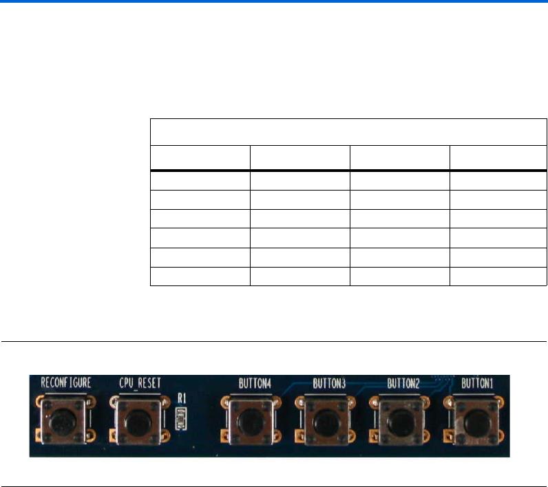
The board has system reset, user reset, and user push-buttons. Table 2–9
lists the pinout for all push-buttons. The push-buttons are in logic “1”
until depressed.
Figure 2–5 shows the push-buttons.
Figure 2–5. Push-Buttons
System Reset Push-Buttons
The system reset push-button starts a reconfiguration of the FPGA from
flash memory.
User Reset Push-Buttons
The user reset push-button is an input to the Cyclone III device. This
push-button is intended to be the master reset signal for the FPGA
designs loaded into the Cyclone III device. The user reset push-button is
connected to the DEV_CLRn pin on the FPGA. The DEV_CLRn setting is a
pin option in the Quartus II software that you must enable to function as
DEV_CLRn instead of a standard I/O.
Table 2–9. Push-Button Pinout
Signal Name FPGA Pin Direction Type
KEY0 F1 Input2.5 V
KEY1 F2 Input2.5 V
KEY2 A10 Input2.5 V
KEY3 B10 Input2.5 V
CPU_RESET_N N2 Input2.5 V
RECONFIGURE H5 (nConfig) Input2.5 V
2–12 Altera Corporation
Cyclone III FPGA Starter Board Reference Manual April 2012
Interfaces
User Push-Buttons
The four user push-buttons are intended for use in controlling FPGA
designs loaded into the Cyclone III device. There is no board-specific
function for these four push-buttons.
LEDs
The board has user LEDs and board-specific LEDs. Table 2–10 lists both
user and board-specific LED pinout. A logic “0” illuminate the LEDs.
Figure 2–6 shows the LEDs.
Figure 2–6. LEDs
User LEDs
Status and debugging signals are driven to the user LEDs from FPGA
designs loaded into the Cyclone III device. There is no board-specific
function for the user LEDs.
Table 2–10. Board LED Pinout
Signal Name FPGA Pin Name Direction Type
LED0 P13 Output2.5 V
LED1 P12 Output2.5 V
LED2 N12 Output2.5 V
LED3 N9 Output2.5 V
Power LED ———
MAX Load LED ———
conf done LED ———
Flash LED ———
HSMC Present LED ———
Altera Corporation 2–13
April 2012 Cyclone III FPGA Starter Board Reference Manual
Board Components and Interfaces
Board Specific LEDs
The power LED illuminates when the board’s power is on and working.
The configuration done LED illuminates when the FPGA is configured.
1 Because of the Quartus II software pin placement rules in
various memory banks, you may only be able to use one or two
of the LEDs with DDR designs.
Configuration done LED: The Conf_Done LED illuminates when
the FPGA is configured with any design.
Flash signal LED: The flash_CE_n LED illuminates when the CE_n
signal to the flash is asserted indicating the flash is being accessed.
Power LED: The power LED illuminates when power is applied to
the board.
Memory
The Cyclone III FPGA starter board includes the following memories:
Parallel flash
DDR SDRAM
SSRAM
Parallel Flash
The Cyclone III starter board has a 8M x 16 low voltage parallel flash.
Table 2–11 lists the parallel flash board reference and manufacturing
information.
Table 2–12 shows the parallel flash signal name, corresponding FPGA
pin, signal direction, type, and board reference U6 flash pin.
Table 2–11. Parallel Flash Manufacturing Information
Board Reference Description Manufacturer Manufacturer Part Number
U6 8M x16 low voltage parallel flash Intel PC28F128P30BF65
Table 2–12. Parallel Flash Memory Pinout (Part 1 of 3)
Signal Name FPGA Pin Direction Type U6 (Flash) Pin
flash_sram_a1 E12 Output2.5 V A1
flash_sram_a2 A16 Output2.5 V B1
flash_sram_a3 B16 Output2.5 V C1
flash_sram_a4 A15 Output2.5 V D1
DK-START-3C25N

Mfr. #:
Manufacturer:
Intel / Altera
Description:
Programmable Logic IC Development Tools FPGA Starter Kit For EP3C25F324
Lifecycle:
New from this manufacturer.
Delivery:
DHL FedEx Ups TNT EMS
Payment:
T/T Paypal Visa MoneyGram Western Union

Products related to this Datasheet