Altera Corporation 1–3
April 2012 Cyclone III FPGA Starter Board Reference Manual
Introduction
Block Diagram
Figure 1–1 shows a functional block diagram of the Cyclone III FPGA
starter board.
Figure 1–1. Cyclone III FPGA Starter Board
Handling the
Board
When handling the board, it is important to observe the following
precaution:
c Static Discharge Precaution—Without proper anti-static handling,
the board can be damaged. Therefore, use anti-static handling
precautions when touching the board.
84
HSMC
4
Switches
4
LEDs
4
Parallel Flash
16MB
SSRAM
1MB
4
USB
Blaster
4
DDR
32MB
42
72
Cyclone III
EP3C25F324
1–4 Altera Corporation
Cyclone III FPGA Starter Board Reference Manual April 2012
Handling the Board
Altera Corporation 2–1
April 2012 Preliminary
2. Board Components and
Interfaces
Board Overview
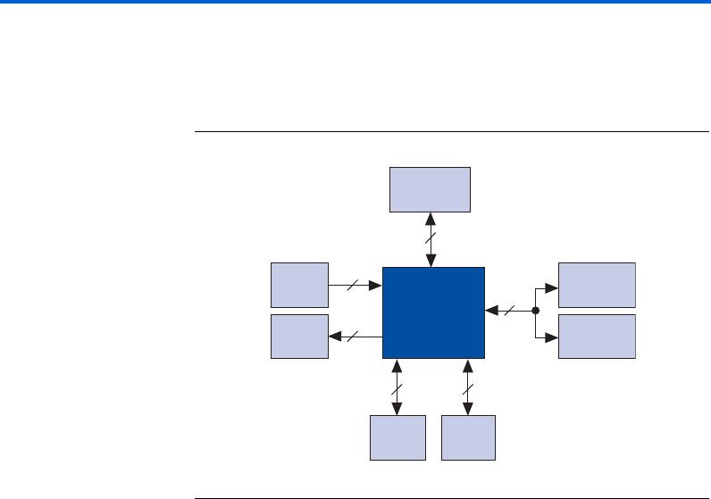
This chapter provides operational and connectivity detail for the board’s
major components and interfaces and is divided into the following major
blocks:
Featured device
Clocking circuitry
Jumpers
Interfaces
USB interface
Altera
®
HSMC expansion connector
General user interfaces
Memory
Power supply
Statement of China-RoHS compliance
1 The board schematics, physical layout database, and
manufacturing files for the Cyclone
®
III FPGA starter board are
included in the Cyclone III FPGA Starter Kit in the following
directory:
<install path>\cycloneIII_3c25_start\board_design_files
f For information on powering-up the Cyclone III FPGA starter board and
installing the demonstration software, refer to the Cyclone III FPGA
Starter Kit User Guide.

DK-START-3C25N

Mfr. #:
Manufacturer:
Intel / Altera
Description:
Programmable Logic IC Development Tools FPGA Starter Kit For EP3C25F324
Lifecycle:
New from this manufacturer.
Delivery:
DHL FedEx Ups TNT EMS
Payment:
T/T Paypal Visa MoneyGram Western Union

Products related to this Datasheet