Altera Corporation 2–17
April 2012 Cyclone III FPGA Starter Board Reference Manual
Board Components and Interfaces
SSRAM
The Cyclone III FPGA starter board has a 256K x 32 synchronous SRAM.
Table 2–15 lists SSRAM board reference and manufacturing
information.
Table 2–16 shows the SSRAM signal name, corresponding FPGA pin,
signal direction, type, and board reference U5 SSRAM pin.
ddr_dq15 V 14 Bidirectional SSTL-2 65
Note to Table 2–14:
(1) The Cyclone III EP3C25F324 only supports one I/O standard in an I/O bank. I/O banks 3 and 4 are shared among
the DDR, HSMC and LEDs. In several DDR designs, some of the I/O pins that share the same banks with the DDR
are unavailable for use due to different I/O standards. Therefore, if you have added DDR to your system, I/O
banks 3 and 4 is to be configured as SSTL-2 only while the HSMC and LEDs pins which are not using SSTL-2,
should be removed.
Table 2–14. DDR SDRAM Pinout (Part 3 of 3) Note (1)
Signal Name FPGA Pin Direction Type U4 (DDR) Pin
Table 2–15. SSRAM Manufacturing Information
Board Reference Description Manufacturer Manufacturer Part Number
U5 256K x 32 synchronous SRAM Integrated Silicon
Solutions, Inc.
IS61LPS25636A-200TQL1
Table 2–16. SSRAM Pinout (Part 1 of 3)
Signal Name FPGA Pin Direction Type U5 (SSRAM) Pin
flash_sram_a2 A16 Output2.5 V 37
flash_sram_a3 B16 Output2.5 V 36
flash_sram_a4 A15 Output2.5 V 35
flash_sram_a5 B15 Output2.5 V 34
flash_sram_a6 A14 Output2.5 V 33
flash_sram_a7 B14 Output2.5 V 32
flash_sram_a8 A13 Output2.5 V 44
flash_sram_a9 B13 Output2.5 V 45
flash_sram_a10 A12 Output2.5 V 46
flash_sram_a11 B12 Output2.5 V 47
flash_sram_a12 A11 Output2.5 V 48
flash_sram_a13 B11 Output2.5 V 49
2–18 Altera Corporation
Cyclone III FPGA Starter Board Reference Manual April 2012
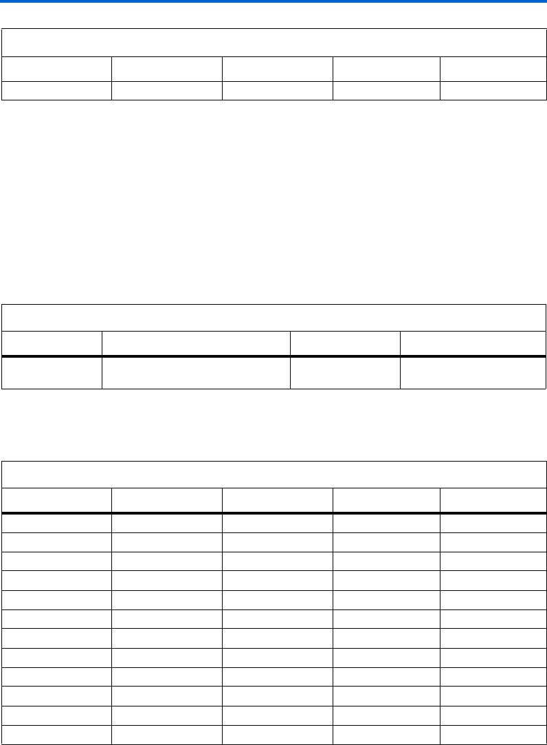
Memory
flash_sram_a14 C10 Output2.5 V 50
flash_sram_a15 D10 Output2.5 V81
flash_sram_a16 E10 Output2.5 V82
flash_sram_a17 C9 Output2.5 V 99
flash_sram_a18 D9 Output2.5 V 100
flash_sram_a19 A7 Output2.5 V 43
flash_sram_a20 A6 Output2.5 V 42
flash_sram_a21 B18 Output2.5 V 39
flash_sram_a22 C17 Output2.5 V 38
flash_sram_dq0 H3 Bidirectional 2.5 V 52
flash_sram_dq1 D1 Bidirectional 2.5 V 53
flash_sram_dq2 A8 Bidirectional 2.5 V 56
flash_sram_dq3 B8 Bidirectional 2.5 V 57
flash_sram_dq4 B7 Bidirectional 2.5 V 58
flash_sram_dq5
C5 Bidirectional 2.5 V 59
flash_sram_dq6 E8 Bidirectional 2.5 V 62
flash_sram_dq7 A4 Bidirectional 2.5 V 63
flash_sram_dq8 B4 Bidirectional 2.5 V 68
flash_sram_dq9 E7 Bidirectional 2.5 V 69
flash_sram_dq10 A3 Bidirectional 2.5 V 72
flash_sram_dq11 B3 Bidirectional 2.5 V 73
flash_sram_dq12 D5 Bidirectional 2.5 V 74
flash_sram_dq13 B5 Bidirectional 2.5 V 75
flash_sram_dq14 A5 Bidirectional 2.5 V 78
flash_sram_dq15 B6 Bidirectional 2.5 V 79
flash_sram_dq16 C16 Bidirectional 2.5 V 2
flash_sram_dq17 D12 Bidirectional 2.5 V 3
flash_sram_dq18 E11 Bidirectional 2.5 V 6
flash_sram_dq19 D2 Bidirectional 2.5 V 7
flash_sram_dq20 E13 Bidirectional 2.5 V8
flash_sram_dq21 E14 Bidirectional 2.5 V 9
flash_sram_dq22 A17 Bidirectional 2.5 V 12
flash_sram_dq23 D16 Bidirectional 2.5 V 13
flash_sram_dq24 C12 Bidirectional 2.5 V 18
Table 2–16. SSRAM Pinout (Part 2 of 3)
Signal Name FPGA Pin Direction Type U5 (SSRAM) Pin
Altera Corporation 2–19
April 2012 Cyclone III FPGA Starter Board Reference Manual
Board Components and Interfaces
Power Supply
The power supply block distributes clean power from the 12 V input
supply to the Cyclone III device through on-board regulators.
To provide various voltage options, the board uses several Linear
Technologies’ regulators. Switching regulators are used for digital circuits
and linear regulators are used for analog circuits. Board regulators are
used to generate the voltages listed in Table 2–17.
flash_sram_dq25 A18 Bidirectional 2.5 V 19
flash_sram_dq26 F8 Bidirectional 2.5 V 22
flash_sram_dq27 D7 Bidirectional 2.5 V 23
flash_sram_dq28 F6 Bidirectional 2.5 V 24
flash_sram_dq29 E6 Bidirectional 2.5 V 25
flash_sram_dq30 G6 Bidirectional 2.5 V 28
flash_sram_dq31 C7 Bidirectional 2.5 V 29
sram_oe_n E9 Output2.5 V86
sram_ce1_n F9 Output2.5 V 98
sram_we_n G13 Output2.5 V87
sram_be_n0 F10 Output2.5 V 93
sram_be_n1 F11 Output2.5 V 94
sram_be_n2 F12 Output2.5 V 95
sram_be_n3 F13 Output2.5 V 96
sram_adsc_n F7 Output2.5 V85
sram_clk A2 Ou
tput2.5 V89
Table 2–16. SSRAM Pinout (Part 3 of 3)
Signal Name FPGA Pin Direction Type U5 (SSRAM) Pin
Table 2–17. Board Regulators
Output
Voltage
(V)
Variance
(+/- mV)
MAX
Current
(A)
Board
Access
Point
Regulator
Board
Reference
Linear
Technologies
Part #
Where Used
1.20 50 3.0 JP6 (1) REG4 LT1959CS8 Cyclone III Core voltage
1.25 50 1.0 JP4 REG2 LTC3413 DDR termination voltage
2.50 50 6.0 JP3 (1) REG1 LTM4603EV DDR, SRAM, Flash, PLLs, other
bias voltages
1.80 80 1.5 JP7 REG5 LT1959CS8 Parallel flash interface, USB buffers
and other I/O

DK-START-3C25N

Mfr. #:
Manufacturer:
Intel / Altera
Description:
Programmable Logic IC Development Tools FPGA Starter Kit For EP3C25F324
Lifecycle:
New from this manufacturer.
Delivery:
DHL FedEx Ups TNT EMS
Payment:
T/T Paypal Visa MoneyGram Western Union

Products related to this Datasheet